Inquire: Call 0086-755-23203480, or reach out via the form below/your sales contact to discuss our design, manufacturing, and assembly capabilities.
Quote: Email your PCB files to Sales@pcbsync.com (Preferred for large files) or submit online. We will contact you promptly. Please ensure your email is correct.
Notes: For PCB fabrication, we require PCB design file in Gerber RS-274X format (most preferred), *.PCB/DDB (Protel, inform your program version) format or *.BRD (Eagle) format. For PCB assembly, we require PCB design file in above mentioned format, drilling file and BOM. Click to download BOM template To avoid file missing, please include all files into one folder and compress it into .zip or .rar format.
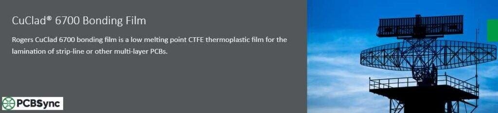
If you’ve spent any time laminating multilayer RF or microwave PCBs with PTFE-based substrates, you’ve probably run into the challenge of finding a bonding material that doesn’t compromise your electrical performance. That’s exactly whereCuClad 6700 Bonding Film comes in.
I’ve worked with various thermoplastic bonding films over the years, and CuClad 6700 remains one of the go-to solutions when you need reliable PTFE-to-PTFE bonding without introducing excessive dielectric loss into your stripline structures. In this guide, I’ll break down everything you need to know—from the technical specs to actual lamination parameters that work on the press.
CuClad 6700 is a chlorotrifluoroethylene (CTFE) thermoplastic copolymer bonding film manufactured by Rogers Corporation. It was specifically developed for laminating stripline and other multilayer circuits built from CuClad, DiClad, or other PTFE-based laminates.
Unlike thermoset prepregs that undergo irreversible chemical curing, CuClad 6700 is a thermoplastic—meaning it softens when heated and solidifies upon cooling. This gives you some flexibility in processing, including the ability to reheat and reflow the bond if needed (though you’ll want to be careful about remelting temperatures during subsequent assembly processes).
Key Characteristics at a Glance
Property
CuClad 6700
Material Type
CTFE Thermoplastic Copolymer
Manufacturer
Rogers Corporation
Primary Use
PTFE substrate bonding in multilayer RF/microwave PCBs
Available Formats
Roll (24″/610mm) and Sheet
Thickness Options
0.0015″ (0.038mm) and 0.003″ (0.076mm)
Space Qualification
NASA/ESA compliant
CuClad 6700 Bonding Film Specifications
Getting the specs right matters when you’re designing a controlled-impedance stackup. Here’s what you’re working with.
Electrical Properties
The electrical characteristics of CuClad 6700 are what make it attractive for high-frequency work. The dielectric constant falls in the midrange of the CuClad and DiClad product families, so you get reasonable Dk matching without introducing significant impedance discontinuities at the bond layer.
Parameter
Value
Test Condition
Dielectric Constant (Dk)
2.30
10 GHz
Dissipation Factor (Df)
0.0025
10 GHz
Volume Resistivity
>10^13 Ω·cm
—
Dielectric Strength
1500 V/mil
ASTM D149
A Dk of 2.30 sits comfortably between many common PTFE laminates, which typically range from 2.17 to 2.60. This means your stripline impedance calculations won’t be thrown off significantly by the bond layer thickness.
Thermal Properties
Thermal behavior is critical for two reasons: the lamination process itself and what happens during downstream assembly (soldering, rework, etc.).
Parameter
Value
Melting Temperature
397°F (203°C)
Bonding Temperature Range
400°F – 475°F
Remelting Temperature
~350°F (177°C)
Thermal Conductivity
0.25 W/m·K
The 397°F melting point means CuClad 6700 is suitable for many applications, but you need to watch your assembly temperatures. If you’re planning on hot air solder leveling (HASL) or wave soldering, the board could see temperatures that approach or exceed the remelt point. For those situations, you might need to consider FEP-based films with higher transition temperatures.
Physical Properties
Parameter
Value
Density
2.1 g/cm³
Water Absorption
<0.02%
Available Thickness
0.0015″ (0.038mm), 0.003″ (0.076mm)
Roll Width
24″ (610mm)
Shelf Life
Unlimited (when stored properly)
The low water absorption is a real benefit. PTFE materials in general don’t absorb much moisture, and the bonding film follows suit. This means your electrical properties stay stable even in humid environments—important for field-deployed RF equipment.
Benefits of Using CuClad 6700 Bonding Film
After working with CuClad 6700 on numerous multilayer builds, here’s what stands out:
Excellent Dk Matching
The dielectric constant of 2.30 aligns well with many PTFE-based laminates. When you’re building a stripline structure, having a bond layer with significantly different Dk would create impedance discontinuities at the layer interfaces. CuClad 6700 minimizes this problem.
Low Outgassing
This is a big deal for aerospace and space applications. Low outgassing means the material won’t release volatile compounds when exposed to vacuum conditions—essential for satellite electronics where outgassed materials can contaminate sensitive optics or solar cells.
CuClad 6700 is compliant with NASA and ESA guidelines for satellite and space applications, which requires meeting strict outgassing criteria.
Shorter Lamination Cycles
Compared to thermosetting prepregs, thermoplastic films like CuClad 6700 require less time at temperature. You’re not waiting for a chemical cure to complete—just heating to flow, maintaining pressure, and cooling. This can improve your press utilization.
Reflow Capability
Because it’s thermoplastic, CuClad 6700 can theoretically be reheated and reflowed. This can be useful if you need to rework a multilayer bond. However, in practice, you’ll want to avoid unintentional reflow during soldering operations.
RoHS Compliant
CuClad 6700 is an environmentally friendly material that meets RoHS standards. No concerns about restricted substances.
Primary Applications for CuClad 6700
Stripline Circuitry
Stripline structures—where the signal trace is sandwiched between two ground planes—are the primary application. The bonding film holds the layers together while contributing minimal electrical loss to the transmission line.
Multilayer Microwave PCBs
Any multilayer construction using PTFE-based cores can benefit from CuClad 6700. This includes hybrid digital/RF boards where you need to integrate high-frequency RF sections with lower-frequency digital or power layers.
Space and Satellite Electronics
The NASA/ESA compliance makes CuClad 6700 a natural choice for space-bound hardware. Satellites, launch vehicles, and space probes all have electronics that need to survive launch vibration, thermal cycling, and vacuum conditions.
Radar Systems
Phased array antennas and other radar components often use PTFE-based multilayer boards. CuClad 6700 provides the bonding solution for these high-reliability applications.
High-Reliability Communication Systems
Military communications, avionics, and other mission-critical systems where failure isn’t an option. The stable electrical properties and proven track record make CuClad 6700 a trusted material in these sectors.
Heat Sink Attachment
Beyond just circuit layers, CuClad 6700 can bond circuit boards to heavy plate heat sinks. This is useful for high-power RF amplifiers where thermal management is critical.
CuClad 6700 vs CuClad 6250: Which One Should You Use?
Rogers offers two bonding films in this family, and choosing between them comes down to your temperature requirements.
Parameter
CuClad 6700
CuClad 6250
Material Chemistry
CTFE copolymer
Ethylene-acrylic acid copolymer
Dielectric Constant
2.30
2.32
Dissipation Factor
0.0025
0.0015
Melting Temperature
397°F (203°C)
213°F (101°C)
Bonding Temperature
450°F (set point)
275°F (set point)
Best For
Higher temp tolerance
Low temp/pressure sensitive substrates
When to Choose CuClad 6700
Your multilayer will see temperatures above 200°F during assembly or operation
You need better thermal margin for soldering processes
The substrates can handle the higher lamination temperatures (400-475°F)
When to Choose CuClad 6250
You’re bonding pressure-sensitive dielectric materials like foam
The substrates can’t tolerate high lamination temperatures
Lower processing temperatures are preferred for your facility
The slightly lower Df of CuClad 6250 (0.0015 vs 0.0025) might seem attractive, but in most practical applications at microwave frequencies, this difference won’t significantly impact system performance.
Lamination Process for CuClad 6700 Bonding Film
Getting a good bond requires attention to the process parameters. Here’s a step-by-step approach based on Rogers’ recommendations and practical experience.
Storage and Handling
Before you even get to the press, proper storage matters:
Store in original sealed packaging
Temperature: Below 25°C (77°F)
Relative humidity: Below 70%
Keep rolls standing upright or suspended by roll cores to prevent flat spots and creases
Handle with gloves in a clean, dust-free environment
One advantage of CuClad 6700: there are no shelf-life limitations when stored properly. Unlike some thermoset prepregs that have limited out-time, this material is stable indefinitely.
Lamination Parameters
Parameter
Recommended Value
Press Set Temperature
450°F (232°C)
Actual Bonding Temperature
400°F – 475°F (min–max)
Pressure
100 psi (up to 200 psi for complex fill)
Hold Time at Temperature
15 minutes minimum
Cool-Down Rate
≤10°F/min
Release Temperature
Below 200°F
Step-by-Step Lamination Process
Step 1: Prepare the Stackup Position the CuClad 6700 film between the layers to be bonded. Make sure you use enough film thickness to encapsulate the copper traces and patterns while providing the required dielectric spacing.
Step 2: Install Thermocouple Place a thermocouple at the edge of the bond line (outside the working circuit area) to monitor actual temperature at the bonding interface. The set temperature on your press is not necessarily what the material sees.
Step 3: Preheat Press Set the press to approximately 450°F. The actual bonding occurs in the 400-475°F range.
Step 4: Apply Pressure Start with 100 psi. If the film doesn’t flow sufficiently to encapsulate complex circuit patterns, you can increase to 200 psi. Use adequate padding to distribute pressure evenly.
Step 5: Hold at Temperature Once the bond line reaches temperature (400°F minimum), hold for at least 15 minutes. Insufficient time at temperature is a common cause of bond failures. Don’t rush this step.
Step 6: Controlled Cool-Down This is critical. Cool under pressure at no more than 10°F per minute. Rapid cooling creates layer-to-layer stress that can cause delamination or warpage.
Step 7: Release Don’t remove from the press until the temperature drops below 200°F.
Common Lamination Mistakes to Avoid
Insufficient hold time: The 15-minute minimum is essential. Spotty or failed bonds are often traced back to inadequate time at temperature.
Cooling too fast: Forced cooling or removing from the press too early leads to warpage and potential delamination.
Contamination: Oils from fingerprints or dust can prevent proper bonding. Always use gloves and work in a clean environment.
Uneven pressure: Without proper padding, some areas may not achieve adequate bonding pressure.
Design Considerations for Engineers
Impedance Calculations
When designing stripline structures with CuClad 6700 as the bonding layer, use Dk = 2.30 for the bond layer in your stackup calculations. Most impedance calculators and field solvers allow you to specify different dielectric constants for each layer.
Layer Thickness Planning
The available thicknesses (0.0015″ and 0.003″) need to be factored into your total dielectric spacing. Remember that some film thickness will flow into the circuit patterns during lamination, so the final bond layer thickness may be slightly less than the starting film thickness.
Thermal Considerations
If your board will see soldering temperatures above 350°F, consider whether the remelt temperature of CuClad 6700 could be a concern. For lead-free soldering with peak temperatures around 260°C (500°F), you’re well above the remelt temperature. In these cases, localized heating (selective soldering) or alternative bonding materials might be necessary.
Useful Resources and Downloads
Here are the key technical resources for working with CuClad 6700:
Rogers also provides calculators and tools for impedance calculation, Dk/Df lookup, and material selection on their Technology Support Hub.
Frequently Asked Questions (FAQs)
Does CuClad 6700 Bonding Film have a shelf life?
No. When stored properly—in the original sealed packaging, below 25°C (77°F), and at less than 70% relative humidity—CuClad 6700 has no shelf-life limitations. This is a significant advantage over thermosetting prepregs, which often have limited storage time.
Can CuClad 6700 be used for sequential lamination?
Thermoplastic bonding films like CuClad 6700 are generally not recommended for sequential lamination processes. The remelt temperature (approximately 350°F) is below typical subsequent lamination temperatures, which could cause previously bonded layers to delaminate. For sequential lamination, consider thermoset options like Rogers 2929 bondply.
Is CuClad 6700 suitable for lead-free soldering?
This depends on your specific process. The remelt temperature of CuClad 6700 is around 350°F (177°C), while lead-free soldering typically peaks above 250°C (482°F). If the entire board reaches these temperatures, you risk delamination. Localized heating methods or selective soldering may work, but careful process validation is required.
What substrates can CuClad 6700 bond?
CuClad 6700 is specifically designed for bonding PTFE-based substrates, including CuClad and DiClad laminates from Rogers. It can also bond other structural and electrical components to dielectric materials. However, it’s not intended for bonding to FR-4 or other thermosetting laminates.
How does CuClad 6700 compare to FEP bonding films?
FEP (fluorinated ethylene propylene) films have a higher transition temperature around 500°F (260°C), making them more suitable for boards that will undergo high-temperature soldering processes. However, FEP also requires higher lamination temperatures. CuClad 6700’s lower processing temperature (450°F vs 550°F+ for FEP) can be an advantage when your substrates are temperature-sensitive.
Conclusion
CuClad 6700 Bonding Film remains a solid choice for multilayer PTFE lamination in RF and microwave applications. Its combination of good electrical properties (Dk 2.30, Df 0.0025), space qualification, and straightforward processing makes it a practical solution for stripline circuits, phased arrays, and other high-frequency assemblies.
The key to success with CuClad 6700 lies in respecting the process parameters—particularly the hold time at temperature and the controlled cool-down rate. Cut corners on either, and you’ll end up with bond failures that show up later as reliability problems.
For applications that will see lead-free soldering or other high-temperature assembly processes, evaluate whether the remelt temperature will be a concern for your specific design. In those cases, FEP or thermoset alternatives might be worth considering.
If you’re specifying materials for your next multilayer RF build, check the Rogers datasheet and consider requesting samples through their online system to validate the material in your actual fabrication process.
Inquire: Call 0086-755-23203480, or reach out via the form below/your sales contact to discuss our design, manufacturing, and assembly capabilities.
Quote: Email your PCB files to Sales@pcbsync.com (Preferred for large files) or submit online. We will contact you promptly. Please ensure your email is correct.
Notes: For PCB fabrication, we require PCB design file in Gerber RS-274X format (most preferred), *.PCB/DDB (Protel, inform your program version) format or *.BRD (Eagle) format. For PCB assembly, we require PCB design file in above mentioned format, drilling file and BOM. Click to download BOM template To avoid file missing, please include all files into one folder and compress it into .zip or .rar format.


