Inquire: Call 0086-755-23203480, or reach out via the form below/your sales contact to discuss our design, manufacturing, and assembly capabilities.
Quote: Email your PCB files to Sales@pcbsync.com (Preferred for large files) or submit online. We will contact you promptly. Please ensure your email is correct.
Notes: For PCB fabrication, we require PCB design file in Gerber RS-274X format (most preferred), *.PCB/DDB (Protel, inform your program version) format or *.BRD (Eagle) format. For PCB assembly, we require PCB design file in above mentioned format, drilling file and BOM. Click to download BOM template To avoid file missing, please include all files into one folder and compress it into .zip or .rar format.
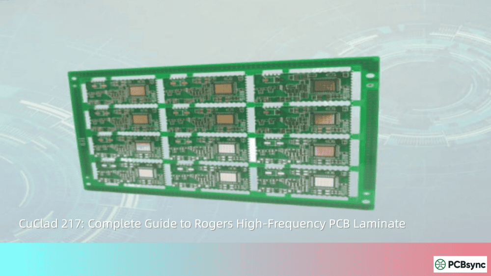
Rogers CuClad 217: Complete Guide to Rogers High-Frequency PCB Laminate
If you’ve spent any time designing RF or microwave circuits, you’ve probably wrestled with material selection. I’ve been there—staring at datasheets, trying to figure out which laminate will actually deliver the performance I need without breaking the bank or causing fabrication headaches. CuClad 217 from Rogers Corporation is one of those materials that keeps coming up in high-frequency design discussions, and for good reason.
This guide covers everything I wish I’d known when I first started working with CuClad 217 PCB substrates—from the technical specs that actually matter in real designs to the fabrication quirks that can save you a failed prototype run.
CuClad 217 is a PTFE (polytetrafluoroethylene) composite laminate reinforced with woven fiberglass, manufactured by Rogers Corporation (originally developed by Arlon, which Rogers acquired). What makes it stand out in the CuClad family is its low fiberglass-to-PTFE ratio, which delivers the lowest dielectric constant (Dk) and dissipation factor available in fiberglass-reinforced PTFE laminates.
The material uses a cross-plied construction where alternating layers of PTFE-coated fiberglass cloth are oriented at 90° to each other. This isn’t just a manufacturing convenience—it provides true electrical and mechanical isotropy in the XY plane. If you’ve worked with phased array antennas or precision filters, you know how critical this isotropy can be for consistent performance across your design.
CuClad 217 Key Material Properties
Here’s a quick reference table of the specifications that matter most for design work:
Property
CuClad 217 Value
Dielectric Constant (Dk) @10 GHz
2.17 or 2.20 (±0.02)
Dissipation Factor (Df) @10 GHz
0.0009
Thermal Coefficient of Er (ppm/°C)
-160
Peel Strength (lbs/inch)
14 (after thermal stress)
CTE (X/Y/Z axis) ppm/°C
29 / 28 / 246
Thermal Conductivity (W/m/K)
0.26
Water Absorption (%)
0.02
Specific Gravity (g/cm³)
2.23
Flammability Rating
UL 94 V-0
Maximum Panel Size
36″ × 36″ (cross-plied)
Why Choose CuClad 217 for Your RF Design?
Ultra-Low Dielectric Loss
That 0.0009 dissipation factor at 10 GHz isn’t just a number on a datasheet—it translates directly to lower insertion loss in your circuits. When you’re designing filters, couplers, or low-noise amplifiers operating at X-band and beyond, every fraction of a dB matters. The low loss tangent means your signal paths maintain integrity without the attenuation that cheaper materials introduce.
Stable Dk Across Frequency
One thing I appreciate about CuClad 217 is how the dielectric constant stays consistent from 1 MHz through 20+ GHz. This stability simplifies the design process significantly—you can scale designs across frequencies without constantly recalculating trace widths or worrying about unexpected impedance shifts. Rogers publishes curves showing this stability, and it holds up in practice.
True XY-Plane Isotropy
The cross-plied construction delivers something no other woven or non-woven fiberglass-reinforced PTFE laminate can claim: genuine electrical and mechanical isotropy in the XY plane. For phased array antenna designers, this eliminates the directional variations that can throw off beam steering calculations and degrade array performance.
Faster Signal Propagation
The low Dk value (2.17) means faster signal propagation compared to higher-Dk materials. Combined with the improved signal-to-noise ratio from low losses, this makes CuClad 217 PCB substrates attractive for timing-critical applications and high-speed digital interfaces that share board space with RF sections.
CuClad 217 Applications: Where This Material Excels
Based on the material properties and real-world deployment, CuClad 217 finds its home in several demanding application areas:
Military and Aerospace Electronics
Radar systems (ground-based, shipboard, and airborne)
Electronic countermeasures (ECM) and electronic support measures (ESM)
Phased array antennas for AESA radar
Satellite communication systems
Missile guidance and tracking systems
Microwave Components
Low-noise amplifiers (LNAs) for sensitive receivers
Bandpass and bandstop filters
Directional couplers and power dividers
Microstrip and stripline transmission lines
Commercial RF Systems
5G infrastructure (base stations, small cells)
Automotive radar sensors (24 GHz, 77 GHz)
Point-to-point microwave links
Test and measurement equipment
CuClad 217 vs. Other Rogers Laminates: How to Choose
Rogers offers a wide portfolio of high-frequency laminates. Here’s how CuClad 217 stacks up against some common alternatives:
Material
Dk @10GHz
Df @10GHz
Best For
Cost
CuClad 217
2.17
0.0009
Lowest loss, isotropy
High
CuClad 233
2.33
0.0013
Balanced performance
Medium
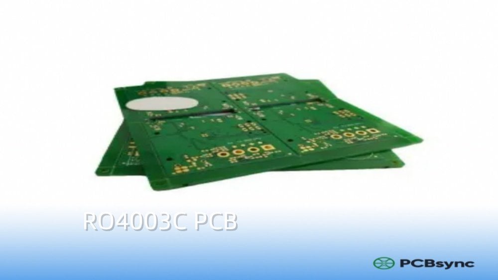
RO4003C
3.38
0.0027
Cost-effective RF
Low
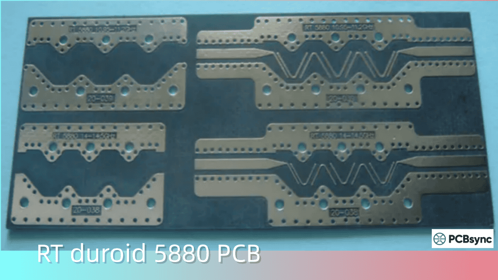
RT/duroid 5880
2.20
0.0009
Aerospace, mmWave
Very High
RO4350B
3.48
0.0037
High-volume commercial
Low-Medium
When to choose CuClad 217: Select CuClad 217 when you need the absolute lowest loss in a mechanically stable PTFE laminate, particularly for precision filters, phased arrays requiring isotropy, or any application where maintaining signal integrity at X-band and above is paramount.
PCB Design Considerations for CuClad 217
Getting the most out of CuClad 217 requires attention to some design details that differ from standard FR-4 practices. The material’s unique properties—particularly its PTFE composition and low Dk value—demand a slightly different approach to layout and stackup planning.
Impedance and Trace Design
Target 50Ω or 75Ω system impedance using appropriate trace width calculators
The low Dk allows wider traces for a given impedance, reducing conductor losses
Use smooth copper foil (1/2 oz or 1 oz ED copper standard) for frequencies above 10 GHz
Rogers recommends controlled impedance tolerance of ±10% for typical applications
Layer Stackup for Multilayer Boards
For multilayer CuClad 217 PCB designs, Rogers offers compatible bondply materials (like Rogers 2929 bondply) that maintain consistent dielectric properties across the stackup. In mixed-dielectric designs, you can combine CuClad for RF sections with standard epoxy laminates for digital circuitry—just be mindful of the CTE mismatch at layer interfaces.
Via Design
Use proper ground via fencing around transmission lines to control impedance
Account for the higher Z-axis CTE (246 ppm/°C) when designing plated through-holes
Consider back-drilling stubs for high-frequency performance
CuClad 217 Fabrication: What Your PCB Shop Needs to Know
PTFE-based laminates like CuClad 217 require specialized fabrication techniques that not every PCB shop has mastered. Before selecting a manufacturer, verify they have documented experience with PTFE materials—the processing differences from FR-4 are significant enough that a shop without proper equipment and procedures can easily ruin expensive material. If you’re working with a PCB manufacturer unfamiliar with PTFE materials, share these guidelines:
Drilling
Use carbide or diamond-coated drill bits designed for PTFE
Control feed rates and spindle speeds to prevent smearing
Stack heights should be limited compared to FR-4 processing
Surface Preparation for Plating
PTFE’s low surface energy creates adhesion challenges. Two proven approaches exist for preparing hole walls:
Sodium etching: Chemical treatment using sodium-based solutions (like Poly-Etch or FluoroEtch) that strips fluorine atoms and creates bondable carbon sites
Plasma treatment: Gas plasma etching increases surface energy for improved adhesion, though typically not as strong as chemical etching
Lamination for Multilayer
Pre-bake PTFE cores at 150-180°C for 1-2 hours to remove moisture
Use vacuum lamination to prevent void formation
Plasma treatment before lamination improves interlayer adhesion
Maintain registration accuracy within ±25 µm for high-frequency multilayers
Surface Finishes
Standard finishes like ENIG, immersion silver, and OSP are compatible with CuClad 217. For applications above 10 GHz, pay attention to surface roughness—smoother finishes help minimize conductor losses at higher frequencies.
CuClad 217 Availability and Ordering
CuClad 217 is available with the following standard options:
Copper cladding: 1/2, 1, or 2 oz electrodeposited copper on both sides; rolled copper available on request
Metal-backed options: Available bonded to aluminum, brass, or copper ground planes for thermal management
Dielectric thickness: Various thicknesses available; specify when ordering
LX testing grade: For critical applications, specify “LX” to have each sheet individually tested with a test report
Useful Resources for CuClad 217
Here are the essential resources for working with CuClad 217:
Interactive comparison tool on Rogers website for filtering and comparing laminates
Sample Request
Request samples through Rogers’ online system at rogerscorp.com
Technical Support
Rogers AES Technical Support: 480-961-1382
Frequently Asked Questions About CuClad 217
Q1: What is the difference between CuClad 217 and RT/duroid 5880?
Both materials offer similar Dk values (~2.2) and extremely low loss tangents (0.0009), but they differ in construction. CuClad 217 uses woven fiberglass reinforcement with a cross-plied structure providing XY isotropy, while RT/duroid 5880 uses random glass microfiber reinforcement. CuClad 217 typically offers better dimensional stability due to the woven glass, while RT/duroid 5880 may be preferred for certain aerospace applications. CuClad 217 is generally more cost-effective than RT/duroid 5880.
Yes. CuClad 217 has a high glass transition temperature (Tg >280°C) and can reliably withstand lead-free reflow and wave soldering processes with peak temperatures up to 260°C. The material’s thermal stability makes it suitable for modern RoHS-compliant manufacturing.
Q3: Is CuClad 217 suitable for outdoor or harsh environment applications?
CuClad 217 exhibits very low moisture absorption (0.02%) and excellent chemical resistance, making it suitable for many outdoor and harsh environment applications. The UL 94 V-0 flammability rating also ensures compliance with safety requirements. For space applications, the material shows low outgassing characteristics (NASA SP-R-0022A compliant).
Q4: What frequencies is CuClad 217 best suited for?
CuClad 217 performs well from low MHz frequencies through millimeter-wave applications (40+ GHz). The stable dielectric constant across frequency and ultra-low loss tangent make it particularly valuable for X-band (8-12 GHz), Ku-band (12-18 GHz), and K-band (18-27 GHz) applications where signal integrity is critical.
Q5: Why would I choose CuClad 217 over cheaper alternatives like RO4003C?
Choose CuClad 217 when your application demands the lowest possible insertion loss, requires XY-plane isotropy (phased arrays), or operates at frequencies where the higher Df of RO4003C would unacceptably degrade performance. For many commercial applications below 10 GHz where cost is a primary concern, RO4003C may indeed be sufficient. CuClad 217 justifies its premium in military, aerospace, and precision instrumentation applications.
One of the standout features of CuClad 217 is its remarkably stable dielectric constant across a wide frequency range. Rogers has published characterization data showing that the Dk varies by less than 1% from 1 GHz to beyond 20 GHz. This stability comes from the precise control of the PTFE-to-fiberglass ratio during manufacturing and the cross-plied construction that eliminates directional Dk variations.
For RF designers, this translates to predictable impedance behavior—what you simulate is what you get on the bench. I’ve seen too many projects stumble because designers assumed their laminate would behave consistently across frequency, only to discover significant Dk shifts that threw off their matching networks. With CuClad 217, you can design a broadband coupler or filter with confidence that the impedances will track across your operating bandwidth.
Thermal Considerations
The thermal coefficient of dielectric constant (TCDk) of -160 ppm/°C deserves attention in temperature-sensitive designs. This negative coefficient means the Dk decreases slightly as temperature increases. For precision applications requiring stable phase response over temperature, you may need to account for this behavior in your design margins.
The thermal conductivity of 0.26 W/m/K is typical for PTFE-based materials—not exceptional, but adequate for most applications. For high-power designs where thermal management is critical, consider the metal-backed variants of CuClad 217 with aluminum, brass, or copper ground planes that provide both mechanical support and improved heat spreading.
Mechanical Properties and Handling
PTFE-based laminates require more careful handling than FR-4. The material is softer and more susceptible to scratching during processing. That said, CuClad 217’s woven fiberglass reinforcement provides better dimensional stability than non-woven alternatives—the cross-plied construction helps resist the warping and distortion that can plague unreinforced PTFE materials during thermal cycling.
When working with this material, avoid mechanical scrubbing of the substrate surface after etching. The copper foil creates a dendrite pattern in the PTFE surface during lamination, and this microstructure is essential for subsequent layer bonding in multilayer builds. Chemical cleaning processes are preferred over mechanical methods to preserve this surface texture.
Signal Integrity Advantages
The combination of low Dk and low Df in CuClad 217 delivers tangible signal integrity benefits. Lower dielectric loss means less signal attenuation per unit length, which is especially important in designs where trace lengths are constrained or where cascaded components accumulate losses. The faster signal propagation enabled by the low Dk can also help in timing-critical applications.
For microstrip designs, the wider trace widths possible with a Dk of 2.17 (compared to FR-4’s ~4.3) also help reduce conductor losses. This is a real advantage at frequencies above 10 GHz where conductor loss becomes the dominant loss mechanism. Smooth copper foil options further reduce skin-effect losses for demanding millimeter-wave applications.
Cost Considerations and ROI
CuClad 217 is a premium material, and there’s no getting around the fact that it costs significantly more than commodity RF laminates like RO4003C. However, the total cost of ownership extends beyond just material cost per square inch.
Consider these factors when evaluating the cost-benefit equation: reduced design iterations due to predictable electrical behavior, lower system-level losses that may eliminate the need for additional amplification stages, and improved reliability in field deployments. For military and aerospace programs where qualification costs and schedule delays are measured in millions, the material premium often pays for itself.
For prototyping, request samples through Rogers’ online system to validate your design before committing to production quantities. Many distributors also stock standard thicknesses, which can reduce lead times for quick-turn prototypes.
Conclusion
CuClad 217 represents the high-performance end of Rogers’ fiberglass-reinforced PTFE laminate portfolio. Its combination of the lowest Dk and Df in its class, true XY-plane isotropy, and proven reliability in demanding military and aerospace applications makes it a go-to choice when signal integrity cannot be compromised.
While not the cheapest option for RF PCB substrates, the performance benefits of CuClad 217 PCB technology often justify the investment—particularly when you factor in reduced design iterations and improved system performance. If you’re designing filters, LNAs, couplers, or phased array systems operating at X-band and beyond, CuClad 217 deserves serious consideration.
For your next high-frequency project, start by downloading the datasheet, running your stackup through Rogers’ impedance calculators, and engaging with a PCB fabricator experienced in PTFE processing. The upfront planning pays dividends in first-pass success. Whether you’re designing military radar systems, commercial 5G infrastructure, or precision test equipment, CuClad 217 offers the electrical performance foundation your demanding applications require.
Inquire: Call 0086-755-23203480, or reach out via the form below/your sales contact to discuss our design, manufacturing, and assembly capabilities.
Quote: Email your PCB files to Sales@pcbsync.com (Preferred for large files) or submit online. We will contact you promptly. Please ensure your email is correct.
Notes: For PCB fabrication, we require PCB design file in Gerber RS-274X format (most preferred), *.PCB/DDB (Protel, inform your program version) format or *.BRD (Eagle) format. For PCB assembly, we require PCB design file in above mentioned format, drilling file and BOM. Click to download BOM template To avoid file missing, please include all files into one folder and compress it into .zip or .rar format.


