Inquire: Call 0086-755-23203480, or reach out via the form below/your sales contact to discuss our design, manufacturing, and assembly capabilities.
Quote: Email your PCB files to Sales@pcbsync.com (Preferred for large files) or submit online. We will contact you promptly. Please ensure your email is correct.
Notes: For PCB fabrication, we require PCB design file in Gerber RS-274X format (most preferred), *.PCB/DDB (Protel, inform your program version) format or *.BRD (Eagle) format. For PCB assembly, we require PCB design file in above mentioned format, drilling file and BOM. Click to download BOM template To avoid file missing, please include all files into one folder and compress it into .zip or .rar format.
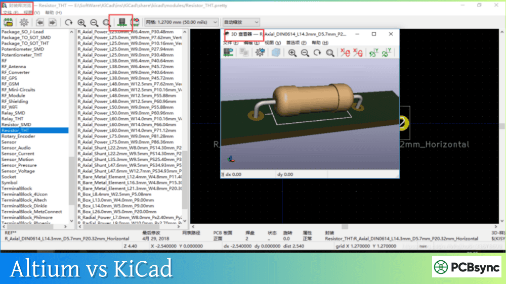
How to Convert KiCad to Altium (and Altium to KiCad): Complete Migration Guide
I’ve been through the PCB tool migration process more times than I’d like to admit. Whether you’re switching jobs, collaborating with teams using different software, or just need to work with reference designs from Texas Instruments or other manufacturers, knowing how to convert KiCad to Altium (and vice versa) is an essential skill for any PCB engineer. This guide covers both directions with practical, tested steps.
Why You Might Need to Convert Between KiCad and Altium
Before diving into the technical steps, let’s address why these conversions happen. In my experience, the most common scenarios include:
Moving from KiCad to Altium: Your company purchased Altium licenses and wants to continue developing existing KiCad projects. Or you landed a job at a company using Altium and want to bring your portfolio designs along.
Moving from Altium to KiCad: You’re leaving a company and can’t take Altium with you. Or you found an excellent reference design in Altium format (many semiconductor vendors provide these) but only have KiCad available. Budget constraints push some startups from Altium to KiCad as well.
Cross-platform collaboration: Your client uses one tool, you use another. Rather than recreating everything from scratch, conversion saves significant time.
The good news? Both tools have improved their import capabilities significantly. KiCad 8 and 9 added native Altium import support, and Altium’s Import Wizard handles KiCad projects reliably.
Supported File Formats at a Glance
Understanding which files can be converted helps you plan your migration strategy.
Version compatibility: Altium Designer 24.6 and later fully supports KiCad 7, 8, and 9 file formats. Older Altium versions may only import KiCad 6 and earlier files.
Altium to KiCad: Supported File Formats
Altium File Type
Extension
KiCad Version
Support Level
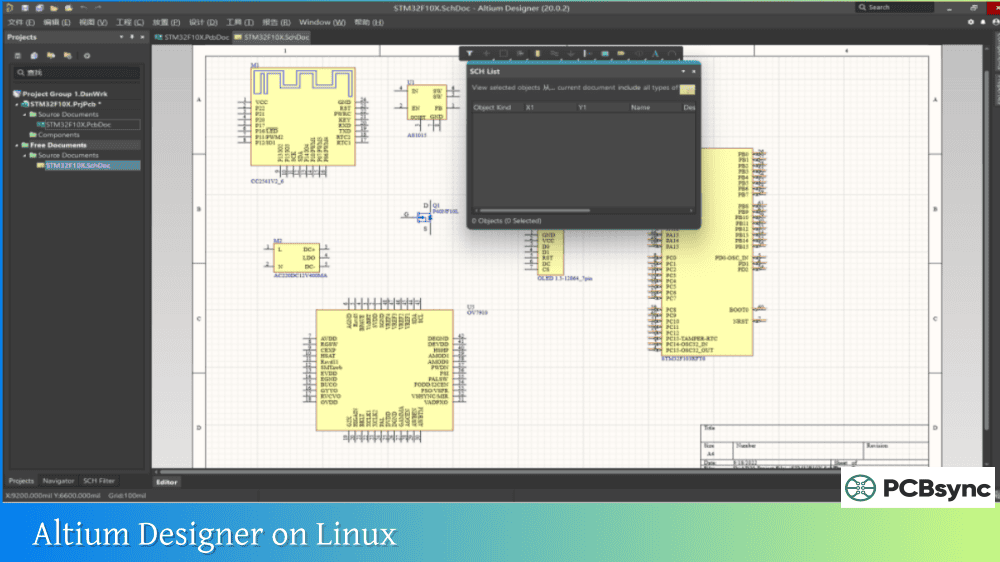
Schematic
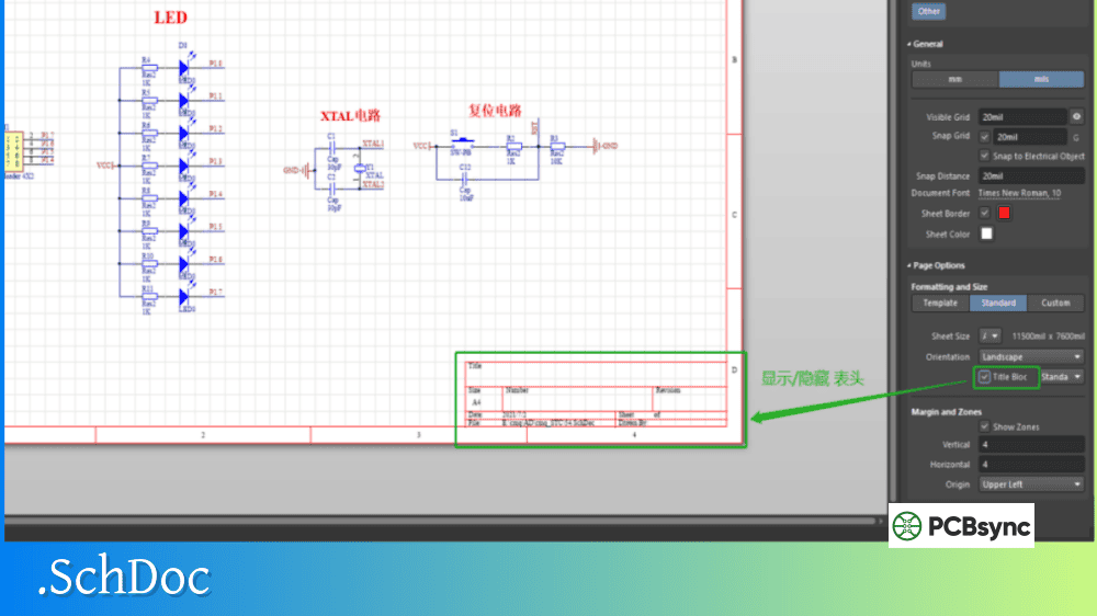
.SchDoc
KiCad 7+
✅ Full support
PCB Layout
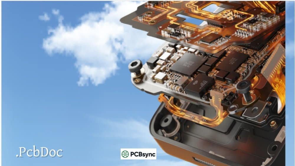
.PcbDoc
KiCad 7+
✅ Full support
Project File
.PrjPcb
KiCad 9.0.3+
✅ New support
Symbol Library
.SchLib
KiCad 8+
✅ Direct use (read-only)
Footprint Library
.PcbLib
KiCad 8+
✅ Direct use (read-only)
Integrated Library
.IntLib
KiCad 8+
✅ Direct use (read-only)
Important note: KiCad 7 and 8 don’t support flat (non-hierarchical) schematics well—each page needs individual import. KiCad 9.0.3 resolves this with project-level import.
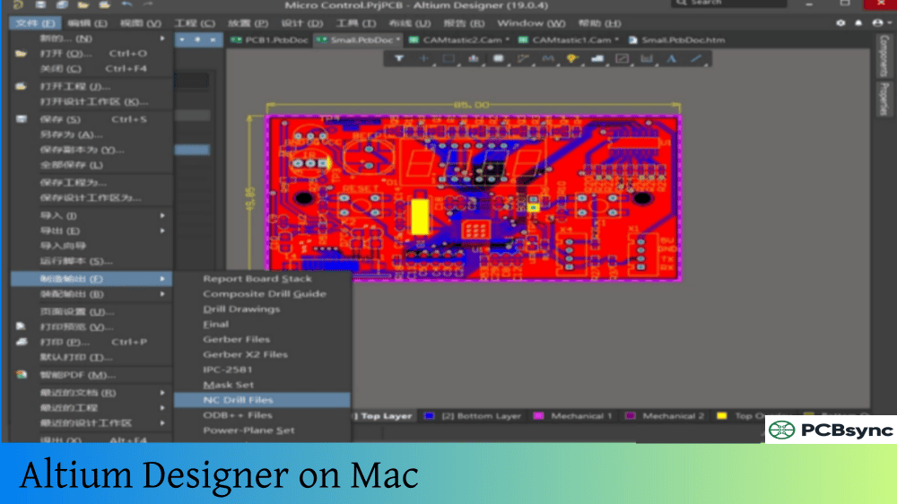
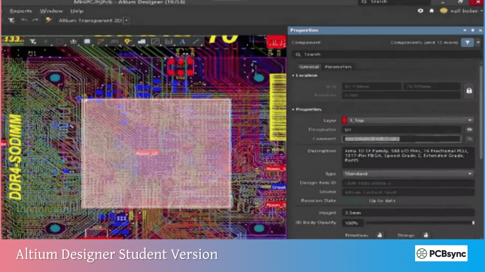
How to Convert KiCad to Altium Designer
The process to convert KiCad to Altium uses Altium’s built-in Import Wizard. Here’s the step-by-step process I follow for every migration.
Step 1: Prepare Your KiCad Project
Before attempting any conversion, clean up your KiCad design:
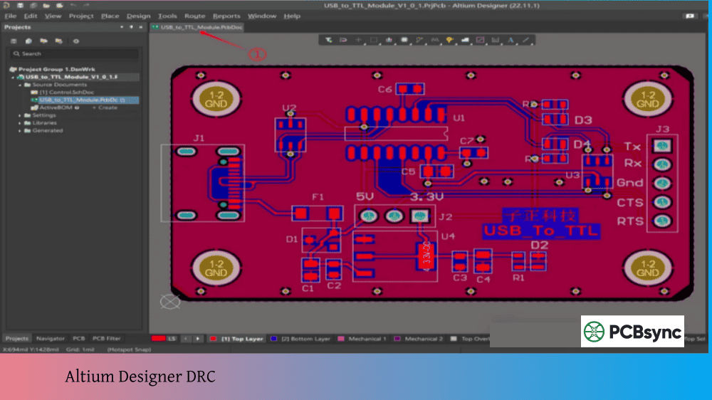
Run DRC (Design Rule Check) and fix all errors
Ensure all footprints are properly assigned to schematic symbols
Update the PCB from schematic to synchronize any changes
Remove any deliberate DRC violations or document them
If using KiCad 6.x, remove dimension objects from the PCB (these can cause import issues)
Files you’ll need: At minimum, gather your .kicad_pro (or .pro), .kicad_sch (or .sch), and .kicad_pcb files. For component libraries, include .kicad_sym and .kicad_mod files as well.
Step 2: Install the KiCad Importer Extension
Altium’s KiCad import capability comes as an extension. To install it:
Open Altium Designer
Click the gear icon in the top-right corner
Select Extensions and Updates
Navigate to Software Extensions
Find KiCad Importer and click the download icon
Restart Altium Designer when prompted
Step 3: Run the Import Wizard
With the extension installed:
Go to File → Import Wizard
Select KiCad Design Files from the list of supported formats
Click Next
Click Add to select your KiCad files (.kicad_sch, .kicad_pcb)
Having your KiCad project open during this step helps verify the layer assignments.
Step 5: Complete Import and Verify
Click Next to run the import. The progress bars show conversion status. When complete:
Review the import log for errors or warnings
Open the generated .SchDoc files and verify schematic accuracy
Open the .PcbDoc file and check:
Board outline integrity
Copper pour/zone fills
Via and pad representations
Design rules (these often need manual adjustment)
Run DRC in Altium to identify any issues
Generate Gerbers and compare against original KiCad Gerbers
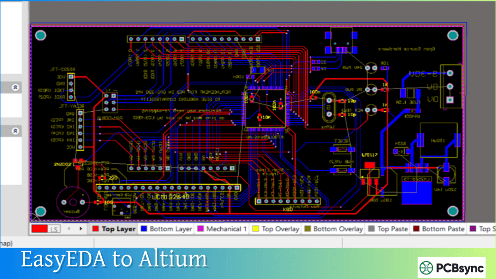
How to Convert Altium to KiCad
Converting Altium projects to KiCad has become significantly easier with KiCad 8 and 9. There are two main approaches: KiCad’s built-in import (recommended) and third-party tools.
Method 1: KiCad’s Native Import (Recommended)
KiCad 7 and later include native Altium import capabilities. KiCad 9 offers the best compatibility.
Importing Altium PCB Files
Open KiCad’s PCB Editor (Pcbnew)
Go to File → Import → Non-KiCad Board File
Change the file filter to Altium Designer (*.PcbDoc)
Select your .PcbDoc file
KiCad processes the file and displays the imported board
Review the import warnings in the dialog
Save as a KiCad .kicad_pcb file
Importing Altium Schematic Files
Open KiCad’s Schematic Editor (Eeschema)
Go to File → Import → Non-KiCad Schematic
Select Altium Designer (*.SchDoc)
Choose your .SchDoc file
For hierarchical designs, select the top-level schematic first—KiCad pulls in sub-sheets automatically
Save as .kicad_sch
For KiCad 9.0.3 and later (project-level import):
Go to File → Import Non-KiCad Project → Altium Project
Select the .PrjPcb file
Choose the output directory
KiCad converts the entire project at once
Importing Altium Libraries Directly
Starting with KiCad 8, you can use Altium libraries without conversion:
Go to Preferences → Manage Symbol Libraries (or Footprint Libraries)
Click the + icon to add a new library
Browse to your .SchLib, .PcbLib, or .IntLib file
Set Library Format to Altium
Give the library a nickname
Click OK
The library is now available in KiCad, though in read-only mode. To edit components, you’ll need to copy them to a native KiCad library.
Method 2: Third-Party Conversion Tools
For older KiCad versions or problematic files, the altium2kicad converter remains useful.
Create a ZIP file containing your .PcbDoc and .SchDoc files (max 40MB)
Upload the ZIP
Download the converted KiCad files
Review the conversionlog.txt for any issues
Local Installation (For Larger Projects)
bash
# Clone the repositorygit clone https://github.com/thesourcerer8/altium2kicad/# Navigate to your Altium project directorycd /path/to/altium/project# Unpack Altium filesperl /path/to/altium2kicad/unpack.pl# Convert schematicsperl /path/to/altium2kicad/convertschema.pl# Convert PCBperl /path/to/altium2kicad/convertpcb.pl
Requirements: Perl must be installed. For 3D model conversion, you’ll also need FreeCAD or the step2wrl tool.
Common Conversion Issues and How to Fix Them
After converting dozens of projects, I’ve encountered these issues repeatedly. Here’s how to resolve them.
Layer Mapping Problems
Symptom: Copper or silkscreen appears on wrong layers after import.
Solution: Carefully verify layer mapping during import. KiCad and Altium use different layer naming conventions. For Altium to KiCad conversions, mechanical layers often map incorrectly—check Mechanical 1 content against Edge.Cuts.
Missing or Broken Footprints
Symptom: Components show as missing footprints or incorrect pad shapes.
Solution: Custom footprints frequently cause issues. After import:
Run DRC to identify missing footprints
Check the import log for footprint warnings
Manually assign correct footprints from your target tool’s libraries
For custom parts, recreate the footprint in the target tool
Design Rules Not Transferred
Symptom: All design rules show default values after import.
Solution: Design rules rarely transfer correctly between tools. Export your original design rules, then manually recreate critical rules (trace width, clearance, via sizes) in the target tool. This actually ensures the rules match your new tool’s manufacturing capabilities.
3D Models Missing
Symptom: 3D view shows missing models for components.
Solution: 3D model paths don’t transfer between tools. You’ll need to:
Export STEP models from the source tool
Convert to WRL format if necessary (KiCad prefers WRL)
Reassign models in the target tool’s footprint properties
Teardrops Causing DRC Errors
Symptom: Numerous DRC violations around vias and pads after Altium to KiCad conversion.
Solution: Remove teardrops in Altium before export, then add them back using KiCad’s teardrop feature after import.
Net Names Changed or Lost
Symptom: Net connectivity appears broken or nets have generic names.
Solution: Hidden pins or implicit connections in schematics cause net issues. Before conversion:
Frequently Asked Questions About KiCad and Altium Conversion
Can I convert KiCad to Altium without an Altium license?
No. The Import Wizard requires a valid Altium Designer license. However, Altium offers a 14-day free trial that includes full import capabilities. If you only need to convert occasionally, the trial period may suffice. For ongoing conversions, you’ll need a subscription or term-based license.
Does converting KiCad to Altium delete my original KiCad files?
No. The conversion creates new Altium files (.SchDoc, .PcbDoc, .PrjPCB) while leaving your original KiCad files completely untouched. You can continue working in KiCad with the original files and have both versions available simultaneously.
Which KiCad version should I use for best Altium import compatibility?
For importing Altium files into KiCad, use KiCad 9 (preferably 9.0.3 or later) for the best compatibility, including project-level import support. KiCad 8 works well for most files but requires importing schematics sheet-by-sheet for flat designs. For converting KiCad to Altium, use Altium Designer 24.6 or later, which supports KiCad 7, 8, and 9 file formats natively.
Are design rules preserved during conversion?
Generally, no. Design rules rarely transfer accurately between PCB tools due to different rule structures and capabilities. Plan to manually configure design rules after any conversion. Export your original rules as documentation, then recreate the critical ones (minimum trace width, clearance, via specifications) in your target tool.
Can I go back and forth between KiCad and Altium on the same project?
Technically yes, but practically it’s problematic. Each round-trip conversion may introduce small errors or require manual cleanup. For active development, choose one tool as your primary platform. If collaboration requires both formats, designate one as the “master” and treat conversions as one-way exports for review purposes only.
Final Recommendations for Successful Conversion
After years of converting designs between these tools, here’s my practical advice:
For KiCad to Altium migrations: The Altium Import Wizard works reliably for most projects. Budget 30-60 minutes for post-import verification and cleanup on typical 4-layer boards. Complex designs with unusual footprints or extensive custom libraries require more attention.
For Altium to KiCad migrations: Use KiCad 9 when possible. The native import handles most designs cleanly. For problematic files, the altium2kicad third-party tool provides an alternative approach. KiCad’s ability to directly use Altium libraries (read-only) simplifies component management significantly.
General best practices:
Always verify converted designs thoroughly before manufacturing
Compare Gerber outputs between original and converted versions
Document any manual fixes for future reference
Keep original files as backups—never overwrite source designs
Converting between KiCad and Altium isn’t perfect, but with careful attention to the process and proper verification, you can successfully migrate projects in either direction without starting from scratch.
Inquire: Call 0086-755-23203480, or reach out via the form below/your sales contact to discuss our design, manufacturing, and assembly capabilities.
Quote: Email your PCB files to Sales@pcbsync.com (Preferred for large files) or submit online. We will contact you promptly. Please ensure your email is correct.
Notes: For PCB fabrication, we require PCB design file in Gerber RS-274X format (most preferred), *.PCB/DDB (Protel, inform your program version) format or *.BRD (Eagle) format. For PCB assembly, we require PCB design file in above mentioned format, drilling file and BOM. Click to download BOM template To avoid file missing, please include all files into one folder and compress it into .zip or .rar format.


