Inquire: Call 0086-755-23203480, or reach out via the form below/your sales contact to discuss our design, manufacturing, and assembly capabilities.
Quote: Email your PCB files to Sales@pcbsync.com (Preferred for large files) or submit online. We will contact you promptly. Please ensure your email is correct.
Notes: For PCB fabrication, we require PCB design file in Gerber RS-274X format (most preferred), *.PCB/DDB (Protel, inform your program version) format or *.BRD (Eagle) format. For PCB assembly, we require PCB design file in above mentioned format, drilling file and BOM. Click to download BOM template To avoid file missing, please include all files into one folder and compress it into .zip or .rar format.
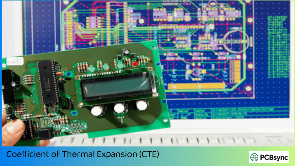
As someone who has spent over a decade troubleshooting field failures and designing reliable circuits, I can tell you that the Coefficient of Thermal Expansion (CTE) is one of the most underestimated factors in PCB design. It’s often overlooked until boards start failing in the field—cracked solder joints, fractured vias, delaminated layers. By then, the damage is done, and redesigning costs time and money.
In this guide, I’ll walk you through everything you need to know about CTE in PCB design, from the fundamental physics to practical material selection strategies that will save your projects from thermal-related failures.
The Coefficient of Thermal Expansion (CTE) measures how much a material expands or contracts when its temperature changes. Every material in existence exhibits this behavior—your house is actually a few inches larger in summer than in winter. In PCB engineering, we express CTE in parts per million per degree Celsius (ppm/°C).
Here’s what that means in practical terms: if you have a PCB that’s 1 million inches long (hypothetically), and it has a CTE of 14 ppm/°C, it would expand by 14 inches for every degree Celsius increase in temperature. Of course, our boards are much smaller, but the principle creates real mechanical stress when different materials with different CTEs are bonded together.
Why CTE Matters in PCB Design
The challenge isn’t that materials expand—it’s that they expand at different rates. A typical FR-4 laminate expands at 14-17 ppm/°C in the X-Y plane, while a silicon chip on that board expands at only 6 ppm/°C. When you heat a 40mm BGA package during reflow soldering, the board underneath it grows more than the package itself. This differential movement creates shear forces on those tiny solder balls, and over repeated thermal cycles, those forces cause fatigue cracks.
I’ve seen countless field returns where the root cause traced back to CTE mismatch. A product works perfectly in the lab, passes qualification testing, then fails after 6 months in an automotive under-hood application where temperature swings between -40°C and +125°C are common.
Understanding CTE Behavior in PCB Materials
X-Y Axis vs. Z-Axis Expansion
PCB materials don’t expand uniformly in all directions. This anisotropic behavior is critical to understand:
X-Y Axis (In-Plane) Expansion: The woven glass fabric in typical FR-4 constrains the epoxy resin, limiting expansion to about 10-20 ppm/°C. This value stays relatively stable even above the glass transition temperature (Tg).
Z-Axis (Through-Thickness) Expansion: Without glass reinforcement in the vertical direction, the resin expands much more freely. Below Tg, you might see 40-60 ppm/°C. Above Tg, this can jump to 200-300 ppm/°C—a five to six times increase.
This dramatic Z-axis expansion is why your plated through-holes (PTHs) crack. The copper barrel inside the via has a CTE of about 17 ppm/°C, while the surrounding laminate might be expanding at 250 ppm/°C during reflow. The copper simply cannot stretch that much, and barrel cracking results.
The Glass Transition Temperature Connection
The relationship between CTE and Tg is fundamental. Below Tg, your laminate behaves predictably with a stable CTE value (called α1). Above Tg, the resin softens and CTE increases dramatically (called α2).
For lead-free soldering with peak temperatures around 260°C, this matters enormously. Standard FR-4 with a Tg of 135°C spends considerable time above its transition point during reflow. High-Tg materials (170°C+) maintain their dimensional stability longer, reducing the accumulated strain on your vias and joints.
CTE Values for Common PCB Materials
Understanding the CTE landscape helps you make informed material decisions. Here’s a comprehensive reference table based on current industry data:
Material
X-Y CTE (ppm/°C)
Z-Axis CTE Below Tg (ppm/°C)
Z-Axis CTE Above Tg (ppm/°C)
Typical Applications
Standard FR-4
14-17
40-60
200-300
Consumer electronics, general purpose
High-Tg FR-4
12-16
35-55
180-250
Lead-free assembly, automotive
Polyimide
12-16
35-50
120-180
High-temperature, aerospace
Rogers RO4000
10-14
30-45
80-120
RF/Microwave, high-frequency
PTFE (Teflon)
70-100
160-200
300+
High-frequency, but requires careful thermal management
Aluminum Nitride (AlN)
4-5
4-5
4-5
High-power LEDs, RF power amplifiers
Alumina (Al₂O₃)
6-8
6-8
6-8
Power electronics, harsh environment
Copper
17
17
17
Traces, vias, pads
Silicon (IC die)
2.6-3
2.6-3
2.6-3
Semiconductor chips
SAC305 Solder
21-23
21-23
21-23
Lead-free solder alloy
Component CTE Reference
When designing for reliability, you need to know what you’re mounting on the board:
Component Type
Typical CTE (ppm/°C)
Mismatch Risk with FR-4
Ceramic BGA (CBGA)
6-8
High
Plastic BGA (PBGA)
12-15
Moderate
Silicon Die
2.6-3
High
MLCC Capacitors (Ceramic)
5-10
Moderate to High
QFN Packages
8-12
Moderate
Leadless Chip Carriers
6-8
High
How CTE Mismatch Causes PCB Failures
Solder Joint Fatigue
This is the most common CTE-related failure mechanism I encounter. During thermal cycling, the PCB expands more than a ceramic BGA package. The solder balls connecting them must accommodate this differential movement through shear deformation. Each cycle adds a small amount of damage—grain growth in the solder, microscopic voids forming at grain boundaries, then micro-cracks linking together until the joint opens completely.
The Coffin-Manson model predicts solder joint life based on this accumulated strain:
Strain Range (Δγ) = C × Δα × ΔT × L / h
Where:
C = correction factor based on temperature and dwell time
Δα = CTE difference between component and PCB
ΔT = temperature swing
L = distance from neutral point to the joint
h = solder joint height
The key takeaway: larger packages, wider temperature swings, and greater CTE mismatch all reduce solder joint life. The outermost corner balls on a large BGA always fail first because they’re farthest from the package center.
Plated Through-Hole (PTH) Cracking
When your board heats past Tg, Z-axis expansion pulls on the copper barrel inside every via. If your copper plating is too thin—anything under 1.0 mil (25μm) is risky—the tensile stress can exceed what the copper can handle. The barrel cracks, usually near the mid-plane where stress concentrates.
High-aspect-ratio vias in thick boards are most vulnerable. IPC Class 3 specifications require minimum 1.0 mil barrel plating for good reason.
Layer Delamination
Excessive CTE mismatch between copper and laminate can generate enough stress during temperature excursions to break the bond between layers. This creates internal gaps that trap moisture, cause impedance shifts, and eventually lead to electrical failures.
Via-to-Pad Separation
In HDI boards with stacked microvias, repeated thermal cycling can cause the via to separate from its landing pad. This failure mode has become more common as designs push the limits of via-in-pad technology.
Strategies for Managing CTE in PCB Design
Material Selection Approaches
For Standard Applications: High-Tg FR-4 (Tg ≥ 170°C) provides a cost-effective improvement over standard materials. The higher transition temperature delays the onset of high Z-axis expansion during lead-free soldering.
For High-Reliability Applications: Consider filled resin systems where ceramic or silica fillers reduce Z-axis CTE to 30 ppm/°C or below. Materials like Isola 370HR or Panasonic Megtron achieve this balance.
For Extreme Thermal Requirements:Metal-core PCBs, ceramic substrates (AlN, Al₂O₃), or specialty laminates with Kevlar/Aramid reinforcement provide CTE values closer to semiconductor silicon.
Design Guidelines to Minimize CTE Effects
Copper Plating Thickness: For through-holes, specify minimum 1.0 mil (25μm) copper. For high-reliability applications, 1.5 oz (1.5 mil) barrel plating can survive 3000+ thermal cycles.
Via Aspect Ratio: Keep aspect ratios below 10:1 for standard processing. Higher ratios concentrate stress and increase failure risk.
BGA Underfill: For large ceramic BGAs, underfill material distributes stress across the entire package footprint rather than concentrating it on individual solder balls.
Thermal Relief Patterns: On large thermal pads, use spoke patterns to reduce the total copper area that must accommodate differential expansion.
Symmetrical Stackups: Ensure your layer stack is balanced around the center to prevent warpage during lamination and reflow.
Reducing Thermal Cycling Exposure
Minimize Reflow Passes: Each reflow cycle above Tg counts against the board’s fatigue life. Design for single-sided reflow where possible.
Control Cooling Rates: Rapid cooling after reflow creates thermal shock. Recommended cooling rates are typically 2-4°C/second to minimize stress.
Operational Thermal Management: Proper heatsinking and thermal vias reduce the temperature swings components experience during operation.
IPC-TM-650 Method 2.6.7: Specifies liquid-to-liquid thermal shock testing. Boards transfer between hot and cold baths with transition times under 10 seconds.
JEDEC JESD22-A104: Defines temperature cycling conditions. Common profiles include -55°C to +125°C for military/aerospace and -40°C to +85°C for industrial.
CTE Measurement Methods
Thermomechanical Analysis (TMA): The standard method for measuring CTE in PCB materials. A probe tracks dimensional change as temperature increases at a controlled rate.
Dilatometry: Measures length change directly and works well for bulk materials.
Microsection Analysis
After thermal cycling, cross-sectioning reveals any barrel cracks, via cracks, or layer separation. This destructive test remains the gold standard for evaluating PTH reliability.
Industry Standards and Specifications
Several IPC standards govern CTE-related requirements:
Standard
Description
IPC-4101
Base material specifications including CTE requirements for various slash sheets
IPC-6012
Qualification and performance specification for rigid boards; defines thermal stress test requirements
IPC-TM-650
Test methods manual including CTE measurement procedures
IPC-9701
Solder joint reliability testing guidelines
IPC-4101 CTE Recommendations
According to IPC-4101, recommended maximum Z-axis CTE values are:
Below Tg: 50-70 ppm/°C
Total Z-axis expansion from 50°C to 260°C: 3.5% maximum for high-reliability applications
Emerging Technologies in CTE Management
Low-CTE Laminate Systems
Material suppliers continue developing composites with improved CTE performance. Aramid fiber reinforcement, ceramic fillers, and modified resin chemistries now achieve Z-axis CTE values below 30 ppm/°C while maintaining reasonable processing characteristics.
Advanced Ceramic Substrates
Aluminum nitride (AlN) represents the cutting edge for high-power applications. With thermal conductivity of 170 W/mK and CTE matching silicon at 4-5 ppm/°C, it eliminates the CTE mismatch problem entirely for direct die attach applications.
Simulation-Driven Design
Modern finite element analysis (FEA) tools can predict stress concentrations and solder joint life before fabrication. This allows designers to optimize pad shapes, via placement, and material selection based on the specific thermal profile the product will experience.
Practical Resources and Databases
Material Datasheets and Databases
IPC Designers Council Resources: ipc.org/resources
Isola Laminate Data Sheets: isola-group.com
Rogers Corporation Material Selector: rogerscorp.com
Many laminate suppliers provide online calculators for estimating stackup CTE based on layer thicknesses and material selections.
Standards Documents
IPC-4101: ipc.org (purchase required)
JEDEC Standards: jedec.org
IPC-TM-650 Test Methods: Available free at ipc.org
Frequently Asked Questions About PCB CTE
What is a good CTE value for PCB materials?
For general applications, X-Y CTE between 12-17 ppm/°C is acceptable. Z-axis CTE below 50 ppm/°C (below Tg) provides good reliability. For high-reliability applications with large ceramic components, targeting X-Y CTE below 12 ppm/°C and matching component CTE as closely as possible reduces failure risk significantly.
How does CTE affect BGA solder joint reliability?
CTE mismatch between the PCB and BGA package causes shear strain in solder balls during temperature changes. Larger packages with greater distance from the neutral point to corner balls experience higher strain. Repeated cycling leads to fatigue cracking, with corner joints typically failing first. Underfill materials can improve joint life by distributing stress across the entire package area.
Why does Z-axis CTE increase above the glass transition temperature?
Below Tg, the epoxy resin matrix is rigid and constrained. Above Tg, the resin transitions to a rubbery state with significantly reduced modulus. Without the mechanical stiffness to resist expansion, the resin expands much more freely in the Z direction—often 3 to 6 times the below-Tg rate. This is why maintaining Tg above peak process temperatures is so important.
Can I use standard FR-4 for automotive applications?
Standard FR-4 with Tg around 135°C is generally not recommended for under-hood automotive applications where temperatures can exceed 125°C. High-Tg FR-4 (170°C+) or polyimide-based materials are better choices. Additionally, materials with reduced CTE and higher thermal stability provide the reliability margins automotive OEMs require.
How do I calculate expected solder joint life based on CTE mismatch?
The Engelmaier model and Coffin-Manson equations provide analytical predictions. You need the CTE values of both the PCB and component, the temperature range the assembly will experience, dwell times at temperature extremes, solder joint geometry, and solder material properties. Many FEA software packages include these calculations, or you can use simplified spreadsheet-based approaches for early design estimates.
Conclusion
Managing Coefficient of Thermal Expansion (CTE) effectively separates robust, reliable PCB designs from those that fail prematurely in the field. The physics are straightforward—materials expand when heated, and different materials expand at different rates. The engineering challenge lies in selecting materials, designing structures, and qualifying processes that accommodate these differences without causing mechanical failures.
As electronic devices continue pushing toward higher power densities, smaller form factors, and more demanding operating environments, CTE management becomes even more critical. The extra attention to material selection and design optimization pays dividends in reduced field failures, lower warranty costs, and satisfied customers.
Whether you’re designing consumer electronics or mission-critical aerospace systems, understanding and controlling CTE-related effects should be a core part of your design process. The resources and guidelines in this article provide a foundation for making informed decisions that improve the thermal-mechanical reliability of your PCB assemblies.
Inquire: Call 0086-755-23203480, or reach out via the form below/your sales contact to discuss our design, manufacturing, and assembly capabilities.
Quote: Email your PCB files to Sales@pcbsync.com (Preferred for large files) or submit online. We will contact you promptly. Please ensure your email is correct.
Notes: For PCB fabrication, we require PCB design file in Gerber RS-274X format (most preferred), *.PCB/DDB (Protel, inform your program version) format or *.BRD (Eagle) format. For PCB assembly, we require PCB design file in above mentioned format, drilling file and BOM. Click to download BOM template To avoid file missing, please include all files into one folder and compress it into .zip or .rar format.


