Inquire: Call 0086-755-23203480, or reach out via the form below/your sales contact to discuss our design, manufacturing, and assembly capabilities.
Quote: Email your PCB files to Sales@pcbsync.com (Preferred for large files) or submit online. We will contact you promptly. Please ensure your email is correct.
Notes: For PCB fabrication, we require PCB design file in Gerber RS-274X format (most preferred), *.PCB/DDB (Protel, inform your program version) format or *.BRD (Eagle) format. For PCB assembly, we require PCB design file in above mentioned format, drilling file and BOM. Click to download BOM template To avoid file missing, please include all files into one folder and compress it into .zip or .rar format.
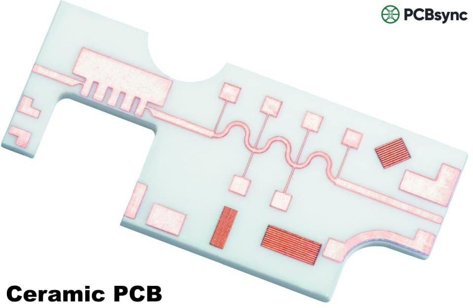
Ceramic PCB: The Complete Guide to Materials, Types, and Applications
When your electronics start generating serious heat, traditional circuit boards hit their limits fast. That’s where ceramic PCBs come in – and they’re changing the game for everything from electric vehicle power modules to high-intensity LED lighting.
If you’re designing products that need to survive extreme temperatures, handle high power, or maintain reliability in harsh environments, understanding ceramic PCB technology isn’t optional anymore. Let’s dive into what makes these boards special, when you actually need them, and how to choose the right one for your project.
A ceramic PCB is a printed circuit board that uses ceramic materials as its base substrate instead of the traditional fiberglass-epoxy (FR4) material you’ll find in most consumer electronics. We’re talking about industrial-grade ceramics like aluminum oxide (Al₂O₃), aluminum nitride (AlN), or silicon nitride (Si₃N₄) – materials that can handle what would literally melt a standard circuit board.
The key difference isn’t just the material itself. In a ceramic PCB, copper traces are directly bonded or plated onto the ceramic surface without needing a separate dielectric insulation layer. This direct contact is what gives ceramic boards their exceptional heat transfer capabilities – there’s simply less material blocking the thermal path.
Think of it this way: FR4 boards are like wearing a thick winter jacket in summer. They trap heat. Ceramic PCBs are more like wearing a moisture-wicking athletic shirt – they pull heat away from where it’s generated and spread it out efficiently.
Why Ceramic PCBs Matter in 2026
The ceramic PCB market is experiencing significant growth, valued at $1.73 billion in 20265 and projected to reach $3.49 billion by 2035. That’s a 7.5% compound annual growth rate driven by real technological needs.
Three major trends are pushing ceramic PCB adoption:
Electric Vehicle Revolution: EV power electronics generate massive amounts of heat. Battery management systems, inverters, and charging stations need boards that won’t fail when currents hit 200A and temperatures soar past 150°C.
High-Power LED Lighting: From automotive headlights to industrial grow lights, LEDs are getting more powerful. A 100W LED array on a standard PCB might last 10,000 hours. Put it on aluminum nitride ceramic, and you’re looking at 50,000+ hours because junction temperatures stay 30-50°C cooler.
5G and Advanced Communications: High-frequency RF circuits running at 10+ GHz need substrates with stable dielectric properties and low signal loss. Ceramic materials deliver both while handling the heat from power amplifiers.
Al₂O₃ (Alumina): Most cost-effective, ideal for general applications. AlN: Best thermal performance, excellent for high-power LEDs and RF. Si₃N₄: Superior mechanical strength, best for thermal cycling reliability. BeO: Highest thermal conductivity but requires special handling (toxic dust). ZrO₂: Excellent for high-temperature sensors and fuel cells.
Note: This is a rough estimate for budgeting purposes. Actual pricing varies based on design complexity, tolerance requirements, and supplier. Lead time: Standard 3-4 weeks, Expedited 1-2 weeks.
✓ DFM Design Rules Checker
Ceramic PCB Design Guidelines
Parameter
DBC
DPC
Thick Film
Thin Film
Min. Line Width
150-200 μm
75-100 μm
100-150 μm
10-25 μm
Min. Line Spacing
150-200 μm
75-100 μm
100-150 μm
10-25 μm
Position Tolerance
±50 μm
±25 μm
±50 μm
±10 μm
Copper Thickness
127-500 μm
35-200 μm
10-50 μm
0.1-5 μm
Via Min Diameter
200 μm
150 μm
200 μm
50 μm
⚙ Ceramic PCB Manufacturing Processes
1
Ceramic Substrate Preparation
High-purity ceramic (Al₂O₃, AlN) substrates are cleaned and prepared. Surface roughness is controlled for optimal bonding.
2
Copper Foil Placement
Oxygen-free copper (OFC) foil is precisely positioned on the ceramic substrate. Both sides can be processed simultaneously.
3
High Temperature Bonding
Assembly heated to 1065-1085°C in controlled atmosphere. Cu-O eutectic forms at interface, creating strong metallurgical bond.
4
Circuit Patterning
Photolithography and chemical etching define circuit patterns. Typical resolution: 150-200μm line/space.
5
Surface Finishing
ENIG, OSP, or other finishes applied. Laser scribing for singulation. Final inspection and testing.
DBC Process Advantages
✓ Excellent thermal conductivity (Cu directly bonded to ceramic)
✓ High current carrying capacity (thick Cu layers 127-500μm)
✓ Superior thermal cycling reliability
✓ No adhesive layer (lower thermal resistance)
✓ Cost-effective for high-power applications
Application Guide
🔌 Power Electronics
IGBT modules, SiC/GaN devices, inverters, converters. Use DBC or AMC with AlN for best thermal performance.
💡 LED & Lighting
High-power LEDs, UV LEDs, automotive lighting. Al₂O₃ DBC offers good balance of cost and performance.
📡 RF & Microwave
Amplifiers, antennas, radar. DPC or thin film on Al₂O₃ for high-frequency applications.
🚗 Automotive
EV power modules, sensors, ECUs. Si₃N₄ for thermal cycling reliability in harsh environments.
Core Materials: The Three Heavyweights
Aluminum Oxide (Al₂O₃) – The Workhorse
Alumina is what most people mean when they say “ceramic PCB.” It’s the most widely used option because it hits a sweet spot between performance and cost.
Key specifications:
Thermal conductivity: 24-30 W/m·K
Operating temperature: Up to 800°C
Dielectric strength: 10-20 kV/mm
Cost: Most affordable ceramic option
Alumina is typically available in 96% and 99.6% purity grades. The 96% version works fine for most LED applications and general power electronics. Go with 99.6% when you need tighter tolerances or better mechanical strength.
Real-world use case: A standard 3W-5W LED module uses aluminum oxide ceramic because the thermal conductivity (still 100x better than FR4) handles the heat load easily, and the cost stays reasonable for mass production.
Aluminum Nitride (AlN) – The Performance Champion
When heat dissipation becomes mission-critical, aluminum nitride steps in. With thermal conductivity ranging from 170-230 W/m·K, it’s in a different league entirely.
Why AlN costs more but performs better:
Thermal conductivity is 6-8x higher than alumina
Coefficient of thermal expansion (2.6-3.5 ppm/°C) matches silicon chips almost perfectly
Reduces mechanical stress during thermal cycling
Extends component lifespan significantly
Here’s where AlN makes business sense: high-power LED truck lights, laser diode systems, EV inverters, and any application where thermal management directly impacts reliability and warranty costs. Yes, you’ll pay 3-5x more than alumina, but you’ll avoid field failures that cost 10x more.
Silicon Nitride (Si₃N₄) – The Tough Specialist
Silicon nitride brings something unique to the table: exceptional mechanical strength combined with good thermal performance (80-120 W/m·K).
Where Si₃N₄ shines:
IGBT modules for electric vehicles
Aerospace and military applications
High-vibration environments
Extreme thermal cycling conditions
The material resists fracture under mechanical shock better than other ceramics, which matters when your PCB is bolted to a vibrating engine block or experiencing repeated heating-cooling cycles.
What About Beryllium Oxide (BeO)?
BeO has incredible thermal conductivity (250-300 W/m·K), but there’s a major problem: beryllium powder is highly toxic during PCB manufacturing. Most companies have phased it out despite its superior performance. You’ll still see it in some legacy aerospace and defense applications, but it’s essentially disappearing from commercial use.
Types of Ceramic PCBs: Manufacturing Matters
The way a ceramic PCB is manufactured fundamentally affects its properties, applications, and cost. Here are the main types:
Direct Bonded Copper (DBC)
DBC technology bonds thick copper foil directly to ceramic substrates at high temperatures (1065-1085°C) in an oxygen-containing nitrogen atmosphere. A copper-oxygen eutectic forms, creating an extremely strong mechanical and thermal bond.
DBC characteristics:
Copper thickness: 100-600 µm (very thick)
High current-carrying capacity
Excellent thermal performance
Circuit precision: Moderate (line width/spacing typically >100µm)
Best for: Power modules, EV inverters, large-scale power electronics
The thick copper in DBC boards handles serious current – we’re talking 100+ amps without breaking a sweat. The trade-off is that you can’t achieve ultra-fine circuit patterns.
Direct Plated Copper (DPC)
DPC uses semiconductor-grade processes: sputtering a thin titanium adhesion layer, then electroplating copper onto the ceramic surface. Circuit patterns are defined through photolithography and etching.
DPC advantages:
Very high circuit precision (down to micron-level features)
Flat surface ideal for high-density components
Thinner copper (typically 25-200 µm)
Better for: High-density LED arrays, RF circuits, precision electronics
When you need to pack hundreds of components into a small space or create complex RF circuits, DPC delivers the precision. However, it can’t match DBC for raw current-carrying capacity.
Active Metal Brazing (AMB)
AMB is the newest technology, using an active metal (often titanium) in the brazing alloy to bond copper to ceramic at high temperatures in a vacuum. This enables copper weights up to 800 µm on thin ceramic substrates.
AMB sweet spot:
Combines thick copper capability with excellent reliability
Superior thermal cycling performance
Ideal for power electronics requiring both high current and thermal stability
Higher cost than DBC or DPC
High-Temperature Co-fired Ceramic (HTCC)
HTCC involves mixing ceramic powder with tungsten or molybdenum pastes, stacking multiple layers, then co-firing everything at 1600-1700°C for 32-48 hours in a hydrogen atmosphere.
HTCC characteristics:
Multilayer capability (complex 3D circuits)
Very high structural strength
Used in aerospace and military applications
Expensive and specialized
Low-Temperature Co-fired Ceramic (LTCC)
LTCC uses glass-ceramic composites fired at around 900°C with gold-based conductive pastes. The lower firing temperature allows for gold metallization, which has excellent conductivity but adds cost.
LTCC applications:
RF modules and filters
Sensor systems
Telecommunications equipment
Medical implantable devices
The ability to embed passive components (resistors, capacitors) directly into LTCC substrates makes them attractive for miniaturization.
Thick Film Ceramic PCB
Thick film boards use screen printing to deposit conductive pastes (silver, gold-palladium) onto ceramic substrates, then sinter at temperatures below 1000°C.
Thick film advantages:
Can integrate passive components directly
Conductor thickness: 10-13 µm
Cost-effective for moderate volumes
Good for hybrid circuits mixing active and passive elements
The Real Performance Numbers
Let’s compare ceramic PCBs against FR4 with actual specifications that matter:
What this means practically: A 100A current trace on an AlN ceramic PCB might see a temperature rise of only 5-17°C depending on trace geometry. That same trace on FR4 would likely delaminate or cause component failure.
Operating Temperature Range
FR4: -50°C to 130°C (standard), up to 170°C (high-Tg variants)
Aluminum Oxide: -55°C to 800°C
Aluminum Nitride: -55°C to 850°C
Silicon Nitride: -40°C to 600°C
Coefficient of Thermal Expansion (CTE)
This number tells you how much the material expands when heated – critical for preventing solder joint failures.
When CTE values match between the PCB and components, mechanical stress stays low during thermal cycling. This dramatically extends reliability, especially in automotive applications experiencing temperature swings from -40°C to 150°C.
Ceramic PCB vs FR4: When to Make the Switch
Here’s the honest truth: FR4 works perfectly fine for most electronics. Ceramic PCBs are specialized tools for specific challenges. So when do you actually need one?
Choose Ceramic PCB When:
1. Thermal management is critical
Power density exceeds 5W/cm²
Components generate concentrated heat spots
Operating temperatures regularly exceed 100°C
External heat sinks aren’t practical due to space constraints
2. High reliability is non-negotiable
Automotive under-hood applications
Aerospace and defense systems
Medical devices where failure has serious consequences
Power levels are moderate (under 3W per component)
Operating temperatures stay below 100°C
Cost is a primary driver
Standard reliability requirements
High-volume consumer products
Real cost comparison:
2-layer FR4 PCB: $2.50-$4.50 USD (volume pricing)
2-layer Al₂O₃ ceramic: $5-$10 USD
2-layer AlN ceramic: $8-$15 USD
That 3-5x cost premium needs justification. But remember: if ceramic prevents warranty returns, extends product lifespan, or eliminates external cooling hardware, the total system cost might actually decrease.
Manufacturing Process: How Ceramic PCBs Are Made
Understanding the manufacturing process helps you design better boards and communicate effectively with manufacturers.
Step 1: Substrate Preparation
Ceramic substrates start as raw powder (Al₂O₃, AlN, etc.) mixed with binders and additives. The mixture is formed into sheets through tape casting – imagine spreading ceramic slurry with a doctor blade to create thin, uniform layers.
For multilayer boards, multiple green (unfired) ceramic sheets are prepared.
Step 2: Via Formation
Holes for interlayer connections are created in the green ceramic sheets either through:
Mechanical punching (for HTCC/LTCC)
Laser drilling (for DPC boards)
CNC drilling (for fired ceramic in DBC process)
Via diameters typically range from 100-300 µm depending on the technology.
Step 3: Metallization
This is where different processes diverge significantly:
For DBC: Copper foil is placed on the ceramic surface and heated to 1070°C in a controlled atmosphere, forming the copper-oxygen eutectic bond.
For DPC: Titanium is sputtered onto the ceramic surface as an adhesion layer, followed by thin copper seed layer deposition, photoresist patterning, electroplating, and etching.
For Thick Film: Silver or gold-palladium paste is screen-printed onto the ceramic and sintered at 850-1000°C.
Step 4: Circuit Formation
Photolithography defines the circuit pattern
Etching removes unwanted metal
Via filling (if needed) creates interlayer connections
Step 5: Finishing
Surface finishes protect exposed metal and ensure solderability:
ENIG (Electroless Nickel Immersion Gold) – most common
The automotive industry represents over 25% of ceramic PCB demand. Key applications include:
Engine Control Units (ECUs): Located near or on the engine block, these operate at 125-150°C continuously with temperature spikes to 175°C. Ceramic PCBs ensure long-term reliability.
LED Headlights: Modern automotive LED headlights use 25-50W per module. Ceramic substrates keep LED junction temperatures below 120°C, ensuring consistent brightness and 25,000+ hour lifespans.
EV Inverters: Converting DC battery power to AC motor drive generates massive heat. Silicon carbide (SiC) power transistors on aluminum nitride ceramic can handle 600V and 200A continuously.
Battery Management Systems: Monitoring individual cells in EV battery packs requires electronics that withstand harsh conditions while maintaining accuracy. Ceramic boards deliver both.
LED Lighting
The LED market is expected to see continued growth with ceramic substrates, particularly for:
High-Power LEDs: Arrays above 50W total power UV LEDs: Sterilization and curing applications using UVC LEDs at 270-285nm wavelengths Horticultural Lighting: Grow lights running 18-24 hours daily need exceptional reliability Stadium and Outdoor Displays: Large format LED screens exposed to direct sunlight and temperature extremes
Case study: A 2025 LED manufacturer reported that switching from aluminum MCPCB to aluminum nitride ceramic extended their truck lamp warranty from 2 years to 5 years while reducing warranty claims by 87%.
Power Electronics
Solar Inverters: Converting DC solar panel output to AC grid power, often in outdoor enclosures that can hit 70°C+ ambient temperatures.
Industrial Motor Drives: Variable frequency drives (VFDs) controlling motors from 1HP to 500HP+ need robust thermal management.
Uninterruptible Power Supplies (UPS): Data centers rely on UPS systems that must maintain reliability over 10-15 year lifespans.
Wireless Charging Stations: High-power wireless EV charging (11-22kW) generates significant heat that ceramic boards efficiently dissipate.
Aerospace and Defense
Radar Systems: Phased array radars use thousands of transmit/receive modules, each generating heat while requiring precise RF performance.
Satellite Communications: Space-qualified ceramics withstand radiation, extreme temperature cycling (-150°C to +150°C), and zero-gravity operation.
Missile Guidance Systems: Extreme acceleration forces and temperature ranges demand the mechanical strength of silicon nitride ceramics.
Avionics: Flight control systems, navigation equipment, and communication systems use ceramic PCBs rated for 30+ year service lives.
Medical Devices
Imaging Equipment: CT scanners, MRI machines, and X-ray systems use high-power electronics that benefit from ceramic thermal management.
Laser Surgical Instruments: Surgical lasers require stable, reliable electronics that won’t fail during procedures.
Implantable Devices: Hermetic ceramic packages protect electronics in pacemakers and neurostimulators.
Telecommunications
5G Base Stations: Power amplifiers for 5G signals (3.5 GHz and mmWave) generate concentrated heat loads. Ceramic substrates prevent thermal throttling.
Optical Network Equipment: High-speed optical transceivers convert between electrical and optical signals at data rates exceeding 100 Gbps.
Design Considerations for Ceramic PCBs
Copper Thickness Selection
Match copper thickness to your current requirements:
0.1mm copper → trace spacing/width should be ≥0.3mm
0.2mm copper → trace spacing/width should be ≥0.4mm
0.3mm copper → trace spacing/width should be ≥0.5mm
Thicker copper carries more current but requires wider spacing and increases costs.
Substrate Thickness
Standard ceramic substrate thicknesses:
0.25mm: Very thin, fragile, used for specialized applications
0.38mm: Thin but manageable
0.63mm: Most common standard
1.0mm: Thick, more robust, better heat spreading
Up to 3.0mm: Special applications requiring mechanical strength
Mechanical Considerations
Ceramics are brittle. Design guidelines:
Avoid sharp corners (use rounded corners with 0.5mm+ radius)
Don’t place mounting holes too close to board edges (minimum 3mm)
Consider board size limitations (typically 138x190mm maximum for single-panel production)
Add stress relief features for connectors and mechanical interfaces
Use compliant materials for mounting (spring-loaded fasteners, rubber grommets)
Thermal Design
Even though ceramic has excellent thermal conductivity, proper thermal design matters:
Calculate thermal resistance: Use the formula θ = t / (k × A)
t = substrate thickness
k = thermal conductivity
A = effective heat spreading area
Plan heat spreading paths: Place high-power components with adequate spacing and orient them to spread heat effectively.
Consider external heat sinking: For extreme power levels (>200W total), ceramic PCBs still benefit from attachment to external heat sinks or cold plates.
Cost Optimization Strategies
Ceramic PCBs cost more, but you can minimize expenses:
Choose the right material: Don’t specify AlN when Al₂O₃ will work. Save that premium for components that actually need it.
Optimize board size: Smaller boards cost less and fit more panels per manufacturing run. Sometimes splitting a design into two smaller ceramic boards with an FR4 interconnect makes economic sense.
Avoid overdesign: Match copper thickness and substrate thickness to actual requirements, not “just to be safe” specs.
Consider hybrid designs: Use ceramic only where needed, FR4 for low-power sections. This works especially well for power supply designs where only the switching stage needs ceramic.
Plan volumes appropriately: Ceramic PCBs have higher NRE (non-recurring engineering) costs but better economies of scale than you might expect. Break-even points vary by complexity but often occur around 500-1000 units.
Work with experienced manufacturers: A good ceramic PCB supplier can optimize your design for manufacturability, potentially saving 20-30% on production costs.
Common Challenges and Solutions
Challenge: Brittle Material
Solution: Design with mechanical strain relief, use compliant mounting, avoid stress concentrators, and handle boards carefully during assembly.
Challenge: Limited Board Size
Solution: If your design exceeds ~190mm in any dimension, consider splitting into multiple boards or using a hybrid approach with ceramic sections connected to FR4.
Challenge: Higher Lead Times
Solution: Ceramic PCBs typically take 2-4 weeks versus 1 week for FR4. Plan accordingly and maintain prototype stock for testing.
Challenge: Assembly Differences
Solution: Reflow temperatures can be higher (up to 260-280°C). Ensure components are rated for these profiles. Some ceramic boards can even handle 400-800°C if needed.
Challenge: Cost Justification
Solution: Build a total cost of ownership model including reliability, warranty costs, field failures, and system-level savings from eliminating external cooling hardware.
Future Trends in Ceramic PCB Technology
Several developments are shaping the future:
Material Innovation: Researchers are developing diamond composite ceramics with thermal conductivities exceeding 1000 W/m·K, though commercial viability remains years away.
Process Fusion: Combining DPC precision with AMB reliability through hybrid processes.
3D Integration: Moving toward embedded components and three-dimensional packaging (3D-IPAC) using ceramic substrates.
Cost Reduction: Mass production and process improvements are gradually reducing ceramic PCB costs. Industry projections suggest 15-20% cost reduction by 2030.
Wider Adoption: As EV and high-power applications grow, ceramic PCBs are transitioning from “specialty” to “standard” in many market segments.
Frequently Asked Questions (FAQs)
1. Can ceramic PCBs be used for flexible applications?
No, ceramic substrates are rigid by nature. If you need flexibility with better thermal performance than standard flex PCB, consider using thin metal-core PCBs or specialized thermal interface materials instead. Ceramic’s strength comes from its crystalline structure, which is inherently inflexible.
2. What’s the typical lead time for ceramic PCB manufacturing?
Lead times vary by manufacturer and technology:
Quick-turn prototypes: 7-10 days (limited options)
Standard production: 2-3 weeks
High-volume orders: 3-4 weeks
HTCC/LTCC multilayer: 4-6 weeks
These timelines are longer than FR4 because of specialized processing equipment and high-temperature firing cycles. Always plan ahead.
3. Can ceramic PCBs be reworked or repaired?
Limited rework is possible but challenging. Because components are often bonded directly to ceramic with high-temperature solder (or even epoxy), removal risks damaging the substrate. Small repairs (replacing a single SMD component) are feasible with proper equipment and expertise. Large-scale rework isn’t practical – it’s usually more cost-effective to replace the board.
4. How do I specify the right ceramic material for my application?
Start with these questions:
What’s your maximum power dissipation? Under 10W total → Al₂O₃ probably works. Over 50W → consider AlN.
What are your operating temperatures? Under 150°C → Al₂O₃ is fine. Over 200°C → AlN or Si₃N₄.
Is vibration a concern? High vibration → Si₃N₄ for fracture resistance.
What’s your budget? Cost-sensitive → start with Al₂O₃.
Most applications actually work fine with aluminum oxide. Don’t over-specify expensive materials unless thermal analysis proves you need them.
5. Are ceramic PCBs environmentally friendly?
Ceramic materials themselves (Al₂O₃, AlN, Si₃N₄) are non-toxic and environmentally stable. The manufacturing process uses less harsh chemistry than FR4 production. However:
Energy consumption is higher due to high-temperature processing
Beryllium oxide (BeO) is toxic during manufacturing (which is why it’s being phased out)
Recycling ceramic PCBs is more difficult than FR4
The longer product lifespans reduce electronic waste
Overall environmental impact depends on the full product lifecycle. The durability and reliability often offset the higher manufacturing energy in high-performance applications.
Valuable Resources for Ceramic PCB Design
To help you implement ceramic PCB technology successfully, here are essential resources:
Technical Standards & Guidelines
IPC-6012 (Class 3): Qualification and performance specification for rigid printed boards, includes ceramic substrates
IPC-A-600: Acceptability of printed boards (visual inspection criteria)
MIL-PRF-55110: Military specification for hybrid microcircuits (covers ceramic substrates)
JESD51: Thermal measurement standards (JEDEC) for semiconductor devices
Ceramic PCBs aren’t a universal solution, but they’re increasingly essential for modern electronics pushing performance boundaries. The key is understanding when their advantages justify the cost premium.
If you’re designing products where thermal management, reliability, or high-frequency performance drive success, ceramic substrates deserve serious consideration. Start with aluminum oxide for most applications, move to aluminum nitride when thermal performance becomes critical, and consider silicon nitride when mechanical robustness matters most.
The market is growing rapidly, costs are gradually decreasing, and manufacturing capabilities continue improving. What was once exotic technology for aerospace is becoming standard practice in automotive and industrial applications.
Take time to analyze your specific requirements, run thermal simulations, and work with experienced ceramic PCB manufacturers. The upfront engineering investment pays off through improved reliability, extended product life, and reduced warranty costs.
Whether you’re designing your first ceramic PCB or optimizing an existing design, understanding the materials, processes, and applications covered in this guide will help you make informed decisions that benefit both performance and profitability.
Ready to move forward with ceramic PCBs? Start by identifying your critical thermal management needs, evaluate material options based on your specific requirements, and engage with qualified manufacturers early in your design process. The future of high-performance electronics is increasingly ceramic – and now you’re equipped to be part of it.
Inquire: Call 0086-755-23203480, or reach out via the form below/your sales contact to discuss our design, manufacturing, and assembly capabilities.
Quote: Email your PCB files to Sales@pcbsync.com (Preferred for large files) or submit online. We will contact you promptly. Please ensure your email is correct.
Notes: For PCB fabrication, we require PCB design file in Gerber RS-274X format (most preferred), *.PCB/DDB (Protel, inform your program version) format or *.BRD (Eagle) format. For PCB assembly, we require PCB design file in above mentioned format, drilling file and BOM. Click to download BOM template To avoid file missing, please include all files into one folder and compress it into .zip or .rar format.


