Contact Sales & After-Sales Service

Contact & Quotation

  • Inquire: Call 0086-755-23203480, or reach out via the form below/your sales contact to discuss our design, manufacturing, and assembly capabilities.
  • Quote: Email your PCB files to Sales@pcbsync.com (Preferred for large files) or submit online. We will contact you promptly. Please ensure your email is correct.
Drag & Drop Files, Choose Files to Upload You can upload up to 3 files.

Notes:
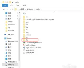
For PCB fabrication, we require PCB design file in Gerber RS-274X format (most preferred), *.PCB/DDB (Protel, inform your program version) format or *.BRD (Eagle) format. For PCB assembly, we require PCB design file in above mentioned format, drilling file and BOM. Click to download BOM template To avoid file missing, please include all files into one folder and compress it into .zip or .rar format.

CAPABILITIES

Rigid PCB Capacity

ItemsMassPrototypes
Layers1-18 Layers PCB1-56 Layers PCB
Max. Panel Size600*770mm( 23.62″*30.31″)600*770mm(23.62″*30.31″) 500*1200mm(19.69″*47.24″)
Max.Board Thickness8.5mm8.5mm
Min. Board Thickness2L:0.3mm2L:0.1mm
4L:0.4mm4L:0.3mm
6L:0.8mm6L:0.6mm
Min Inner Layer Clearance3mil3mil
Min Line width3/3 mil3/3 mil
Min Line space3/3 mil3/3 mil
Min.Hole Size0.1mm0.1mm
Min plated hole thickness25um25um
Min Blind/Buried hole size0.1mm0.1mm(1-18layers)
PTH Dia. Tolerance±0.076mm(±3mil)±0.076mm(±3mil)
Non PTH Dia. Tolerance±0.05mm(±2mil)±0.05mm(±2mil)
Hole Position Deviation±0.05mm(±2mil)±0.05mm(±2mil)
Heavy Coppe4OZ/140μm6OZ/175μm
Min S/M Pitch0.1mm (4mil)0.1mm (4mil)
Soldermask colourGreen,black,Blue,White,Yellow,RedGreen,black,Blue,White,Yellow,Red
Silkscreen colourWhite,Yellow,Red,BlackWhite,Yellow,Red,Black
OutlineRouting,V-Groove, Beveling punchRouting,V-Groove, Beveling punch
Outline Tolerance±0.15mm ±6mil±0.15mm (±6mil)
Peelable maskTop,bottom,double sidedTop,bottom,double sided
Controlled Impedance+/- 10%+/- 7%
Insulation Resistance1×1012Ω(Normal)1×10¹²Ω(Normal)
Through Hole Resistance<300Ω(Normal)<300Ω(Normal)
Thermal Shock3×10sec@288℃3×10sec@288℃
Warp and Twist≤0.7%≤0.7%
Electric Strength>1.3KV/mm>1.4KV/mm
Peel Strength1.4N/mm1.4N/mm
Solder Mask Abrasion>6H>6H
Flammability94V-094V-0
Test Voltage50-330V50-330V

Manufacturing Process Excellence

PCBsyn’s flex PCB manufacturing process encompasses several sophisticated steps, each executed with precision:

  1. Design Optimization: Every successful project begins with a thorough design phase that considers expansion and contraction requirements for long-term durability without breakage.
  2. Material Selection: Choosing appropriate flexible base materials and copper foil conductors based on specific application needs.
  3. Photolithography: Creating precise circuit patterns with advanced imaging techniques.
  4. Chemical Processing: Etching, plating, and cleaning to form the circuit elements.
  5. Lamination: Carefully aligning and bonding layers using heat and pressure to create strong connections while maintaining flexibility in designated areas.
  6. Drilling and Plating: Creating and metallizing holes for interconnections between layers.
  7. Final Fabrication: Cutting and shaping the board to its final form, followed by comprehensive testing and quality assurance.

Applications Across Industries

PCBsyn’s flex PCBs power innovation across numerous sectors:

  • Medical Devices: Implantable devices, wearable health monitors, diagnostic equipment
  • Automotive Electronics: Engine control units, dashboard displays, sensor systems
  • Consumer Electronics: Smartphones, cameras, wearable technology
  • Aerospace: Satellite systems, aircraft control panels, navigation equipment
  • Industrial Control: Automation systems, sensing devices, control interfaces
  • Telecommunications: Network equipment, mobile devices, transmission systems

Advantages of PCBsyn Flex PCBs

Choosing PCBsyn for your flex PCB needs delivers numerous benefits:

  1. Space and Weight Optimization: Our flex and rigid-flex PCBs eliminate the need for connectors and cables, reducing overall system size and weight while enabling more efficient use of available space.
  2. Enhanced Reliability: Flex PCBs have less chance of creating physical connections between board parts, increasing reliability while allowing continuous modification to meet application needs.
  3. Design Flexibility: Our 3D design capabilities allow circuits to conform to unique form factors and tight spaces with shorter signal paths and controlled impedance throughout the assembly.
  4. Thermal Management: Improved heat dissipation compared to traditional rigid boards.
  5. Vibration Resistance: Flex sections reduce strain on solder joints, providing better durability in high-vibration environments.
  6. Cost Efficiency: While individual unit costs may vary based on design complexity, production volume, and turnaround time, our high-volume manufacturing capabilities deliver excellent value.

Quality Assurance and Certifications

PCBsyn maintains strict quality control protocols throughout the manufacturing process:

  • UL Certification for both rigid and flex PCB production
  • ISO compliance for quality management systems
  • Comprehensive environmental and reliability testing
  • Rigorous electrical performance verification

Customer-Centric Approach

At PCBsyn, we understand that flexibility and customer relationships are as important as advanced engineering skills. We provide high-end engineering and manufacturing services tailored to specific requirements, from quick-turn prototyping starting at just 1 piece to volume fabrication.

Future Innovations

PCBsyn continues to pioneer advancements in flex PCB technology, including increased layer counts, integration of new flexible and durable materials, embedding components within PCB layers for increased density, and developing more sophisticated design tools for complex flexible PCB layouts.

Conclusion

With almost two decades of expertise in flex PCB manufacturing, PCBsyn delivers world-class flexible circuit solutions that combine innovative design, precision manufacturing, and exceptional reliability. Our comprehensive capabilities—from simple single-layer designs to complex multi-layer and rigid-flex configurations—enable customers to push the boundaries of electronic product development across industries. Partner with PCBsyn for your flex PCB needs and experience the perfect balance of technological excellence and customer satisfaction.

Flex PCB Manufacturing Capability

DigiKey is the go-to distributor for certified industrial safety solutions across all sectors, including food and beverage, oil and gas, material handling, and more. We cover everything from safety PLCs to personal protective equipment.

Item Description
Layer Flexible board: 1-12Layers Flex-Rigid Board: 2-32Layers
Material PI, PET, PEN, FR-4,dupont
Stiffeners FR4, Aluminum, Polyimide, Stainless Steel
Final Thickness Flexible board: 0.002″ – 0.1″ (0.05-2.5mm) Flexible-rigid board: 0.0024″ – 0.16″ (0.06-4.0mm)
Surface Treatment Lead-free: ENG Gold; OSP, Immersion silver, Immersion Tin
Max / Min Board Size Min: 0.2″x0.3″  Max: 20.5″x13″
Min Trace Width / Min Clearance Inner: 0.5oz: 4/4mil  Outer: 1/3oz-0.5oz: 4/4mil 1oz: 5/5mil               1oz: 5/5mil 2oz: 5/7mil               2oz: 5/7mil
Min Hole Ring Inner: 0.5oz: 4mil     Outer: 1/3oz-0.5oz: 4mil 1oz: 5mil                  1oz: 5mil 2oz: 7mil                  2oz: 7mil
Copper Thickness 1/3oz – 2oz
Max / Min Insulation Thickness 2mil/0.5mil (50um/12.7um)
Min Hole Size and Tolerance Min hole: 8mil Tolerance: PTH±3mil, NPTH±2mil
Min Slot 24mil x 35mil (0.6×0.9mm)
Solder Mask Alignment Tolerance ±3mil
Silkscreen Alignment Tolerance ±6mil
Silkscreen Line Width 5mil
Gold Plating Nickel: 100u” – 200u” Gold: 1u”-4u”
Immersion Nickel / Gold Nickel: 100u” – 200u” Gold: 1u”-5u”
Immersion Silver Silver: 6u” – 12u”
OSP Film: 8u” – 20u”
Test Voltage Testing Fixture: 50-300V
Profile Tolerance of Punch Accurate mould: ±2mil
Ordinary mould: ±4mil
Knife mould: ±8mil
Hand-Cut: ±15mil

Manufacturing Process Excellence

PCBsyn’s flex PCB manufacturing process encompasses several sophisticated steps, each executed with precision:

  1. Design Optimization: Every successful project begins with a thorough design phase that considers expansion and contraction requirements for long-term durability without breakage.
  2. Material Selection: Choosing appropriate flexible base materials and copper foil conductors based on specific application needs.
  3. Photolithography: Creating precise circuit patterns with advanced imaging techniques.
  4. Chemical Processing: Etching, plating, and cleaning to form the circuit elements.
  5. Lamination: Carefully aligning and bonding layers using heat and pressure to create strong connections while maintaining flexibility in designated areas.
  6. Drilling and Plating: Creating and metallizing holes for interconnections between layers.
  7. Final Fabrication: Cutting and shaping the board to its final form, followed by comprehensive testing and quality assurance.

Applications Across Industries

PCBsyn’s flex PCBs power innovation across numerous sectors:

  • Medical Devices: Implantable devices, wearable health monitors, diagnostic equipment
  • Automotive Electronics: Engine control units, dashboard displays, sensor systems
  • Consumer Electronics: Smartphones, cameras, wearable technology
  • Aerospace: Satellite systems, aircraft control panels, navigation equipment
  • Industrial Control: Automation systems, sensing devices, control interfaces
  • Telecommunications: Network equipment, mobile devices, transmission systems

Advantages of PCBsyn Flex PCBs

Choosing PCBsyn for your flex PCB needs delivers numerous benefits:

  1. Space and Weight Optimization: Our flex and rigid-flex PCBs eliminate the need for connectors and cables, reducing overall system size and weight while enabling more efficient use of available space.
  2. Enhanced Reliability: Flex PCBs have less chance of creating physical connections between board parts, increasing reliability while allowing continuous modification to meet application needs.
  3. Design Flexibility: Our 3D design capabilities allow circuits to conform to unique form factors and tight spaces with shorter signal paths and controlled impedance throughout the assembly.
  4. Thermal Management: Improved heat dissipation compared to traditional rigid boards.
  5. Vibration Resistance: Flex sections reduce strain on solder joints, providing better durability in high-vibration environments.
  6. Cost Efficiency: While individual unit costs may vary based on design complexity, production volume, and turnaround time, our high-volume manufacturing capabilities deliver excellent value.

Quality Assurance and Certifications

PCBsyn maintains strict quality control protocols throughout the manufacturing process:

  • UL Certification for both rigid and flex PCB production
  • ISO compliance for quality management systems
  • Comprehensive environmental and reliability testing
  • Rigorous electrical performance verification

Customer-Centric Approach

At PCBsyn, we understand that flexibility and customer relationships are as important as advanced engineering skills. We provide high-end engineering and manufacturing services tailored to specific requirements, from quick-turn prototyping starting at just 1 piece to volume fabrication.

Future Innovations

PCBsyn continues to pioneer advancements in flex PCB technology, including increased layer counts, integration of new flexible and durable materials, embedding components within PCB layers for increased density, and developing more sophisticated design tools for complex flexible PCB layouts.

Conclusion

With almost two decades of expertise in flex PCB manufacturing, PCBsyn delivers world-class flexible circuit solutions that combine innovative design, precision manufacturing, and exceptional reliability. Our comprehensive capabilities—from simple single-layer designs to complex multi-layer and rigid-flex configurations—enable customers to push the boundaries of electronic product development across industries. Partner with PCBsyn for your flex PCB needs and experience the perfect balance of technological excellence and customer satisfaction.

PCBsyn Rigid Flex PCB Capability

Request Flex PCB manufacturing quotation, Pls send PCB files to Sales@PCBsync.com

Rigid-Flex PCB Capabilities

PCBsyn’s rigid-flex PCB manufacturing capabilities represent an impressive blend of technological advancement and precision engineering. As a specialized rigid-flex PCB manufacturer, PCBsyn offers cutting-edge solutions that integrate rigid and flexible substrates into unified, three-dimensional circuit designs.

Layer Capacity

PCBsyn has continuously invested in research and development to enhance its manufacturing capabilities. The company has achieved remarkable milestones in rigid-flex PCB production:

  • Up to 32 layers in rigid sections
  • Up to 12 layers in flexible sections
  • Capability to produce complex rigid-flex designs with various layer combinations
  • Custom stackup configurations based on specific application requirements

This extensive layer capacity allows PCBsyn to accommodate highly complex circuit designs in compact, three-dimensional spaces, making them ideal for applications where space optimization is crucial.

Technical Specifications

PCBsyn’s rigid-flex PCBs are characterized by precise technical specifications:

  • Line width/spacing: As fine as 3mil/3mil (0.076mm/0.076mm)
  • Mechanical drilling: Down to 0.15mm
  • Laser drilling: Down to 0.1mm
  • Board thickness options: Customizable based on application requirements
  • Copper thickness: Standard 1oz, with options for varying copper weights
  • Material options: High-quality substrates including IT180A, AK, and other specialized materials

Material Excellence

PCBsyn utilizes premium materials for both rigid and flexible sections of their rigid-flex PCBs:

Rigid Sections:

Flexible Sections:

  • Polyimide
  • Adhesiveless substrates
  • Custom flexible materials based on application requirements
PCB attributesFlexRigid-flex
Min Layer Count11
Max Layer Count12≤ 32
Min Core thickness.001″ (.025 mm)3 oz (89 ml)
Max Finished Copper Weight (I/L)2 oz (59 ml)3 oz (89 ml)
Max Finished Copper thickness (O/L)12 micron (.012 mm)9 micron (.009 mm) (only for O/L)
Max Panel Size12×1812×18
Smallest Mechanical Drill Diameter.0079″ (.201 mm).0071″ (.180 mm)
Smallest Laser Drill DiameterNo.005″ (.127 mm)
Min Finished Hole Size.006″ (.152 mm).006″ (.152 mm)
Max through Hole Aspect Ratio10:110:1
Max Blind Via Aspect Ratio.75:1.75:1
Min Trace and Space≥ .0035”(.089 mm)≥ .0035”(.089 mm)(rigid)
Min Pad Size for Test.016″ (.406 mm).005” (.127 mm) (rigid)
Process Pad DiameterD + .014″ (.356 mm) (1-mil (.025 mm) annular ring)D + .014″ (.356 mm) (1-mil (.025 mm) annular ring)
Stacked ViasNoNo
Min Wire Bond Pad Size> .006″ (.152 mm)> .006″ (.152 mm)
Controlled Impedance Tolerance10%5%
Solder Mask RegistrationWithin .002″ (.051 mm)Within .002″ (.051 mm)
Solder Mask Feature Tolerance.001″ (.025 mm).001″ (.025 mm)
Solder Mask Min Dam Size.004″ (.102 mm).001″ (.025 mm)
Min Diameter Route Cutter Available.019″ (.483 mm).024″ (.610 mm)
Mechanical Routed Part Size Tolerance.003″ (.076 mm).010″ (.254 mm)
Bow and Twist ToleranceN/AAs per spec
Thickness Tolerance+/- .002″ (.051 mm)10%
Sequential LaminationsN/A2
Buried ViasYesYes
Blind ViasYesYes
Conductive Filled ViasNoYes
Non Conductive Filled ViasNoYes

Manufacturing Process

PCBsyn’s manufacturing process for rigid-flex PCBs involves several sophisticated steps:

  1. Material Selection and Cutting: Precise preparation of rigid and flexible materials
  2. Layer Preparation: Individual layer processing with careful attention to detail
  3. Lamination: Integration of rigid and flexible sections using specialized techniques
  4. Drilling and Plating: Creation of vias and through-holes with high precision
  5. Pattern Transfer: Accurate circuit pattern application
  6. Etching: Controlled removal of unwanted copper
  7. Surface Finish Application: Options include ENIG, immersion tin, and other finishes
  8. Cutting and Shaping: Final forming of the board
  9. Creation of Score Lines: For later folding if required
  10. Rigorous Quality Testing: Ensuring peak performance and reliability

Stackup Configurations

PCBsyn offers various standard and custom stackup configurations for rigid-flex PCBs:

  • 4-Layer Configurations: Typically featuring 2 rigid and 2 flex layers, suitable for simpler designs
  • 6-Layer Configurations: Often with 4 rigid and 2 flex layers, balancing complexity and flexibility
  • 8-Layer Configurations: With 4 flex and 4 rigid layers, offering high circuit density
  • 10-Layer Configurations: Providing very high circuit density with optimized signal routing
  • 12-Layer Configurations: Maximum circuit density for the most complex applications

Each stackup is carefully designed to balance factors such as signal integrity, mechanical stability, flexibility requirements, and thermal management.

Assembly Capabilities

PCBsyn provides comprehensive rigid-flex PCB assembly services, offering a complete solution from design to finished product:

  • Component placement on rigid sections using advanced pick-and-place equipment
  • Various soldering technologies including reflow, wave, and selective soldering
  • Thorough cleaning processes to remove contaminants
  • Comprehensive inspection using AOI, X-ray, and functional testing
  • Optional conformal coating application for environmental protection
  • Full turnkey services including component sourcing

Applications and Industry Solutions

PCBsyn’s rigid-flex PCBs are employed across numerous industries and applications:

Aerospace and Defense

  • Ruggedized designs for extreme conditions
  • High-reliability systems requiring minimal interconnections
  • Compact avionics systems

Medical Devices

  • Ultra-thin, biocompatible designs for implantable devices
  • Patient monitoring equipment
  • Diagnostic systems requiring high signal integrity

Consumer Electronics

  • Smartphones and wearables
  • Digital cameras and CCTV systems
  • Compact consumer devices requiring 3D packaging

Automotive Electronics

  • Vehicle camera systems
  • Engine control units
  • Dashboard electronics and infotainment systems

Industrial Control

  • Factory automation equipment
  • Robotic systems
  • Instrumentation and measurement devices

Communications

  • Telecommunication equipment
  • Network infrastructure
  • RF and microwave systems

Design Considerations and Support

PCBsyn provides comprehensive design support for rigid-flex PCB projects:

  • Expert consultation on stackup design
  • Material selection guidance
  • Design for manufacturing (DFM) review
  • Signal integrity analysis
  • Thermal management solutions
  • Mechanical stress and reliability analysis

PCBsyn’s engineering team works closely with customers to optimize designs for manufacturability, reliability, and cost-effectiveness.

Competitive Advantages

PCBsyn’s rigid-flex PCB capabilities are distinguished by several key advantages:

  • Technological Leadership: Continuous investment in innovative manufacturing techniques
  • Quality Assurance: UL certification and rigorous quality control processes
  • Scalability: Capabilities ranging from quick-turn prototypes to volume production
  • Comprehensive Services: From design assistance to turnkey assembly
  • Cost-Effectiveness: Competitive pricing for both prototyping and production
  • Customer Communication: Responsive service throughout the production process

Conclusion

PCBsyn Technology stands at the cutting edge of rigid-flex PCB manufacturing, offering advanced capabilities, exceptional quality, and comprehensive services. With its extensive experience, technical expertise, and commitment to innovation, PCBsyn provides reliable solutions for even the most challenging rigid-flex PCB applications. Whether for complex aerospace systems, miniaturized medical devices, or next-generation consumer electronics, PCBsyn’s rigid-flex PCB capabilities enable engineers to create sophisticated, space-efficient electronic designs that meet the demands of modern technology.

For specific inquiries or to request a quotation for rigid-flex PCB manufacturing, customers can contact PCBsyn directly at Sales@PCBsync.com.

PCBsync HDI PCB Capability

Request Flex PCB manufacturing quotation, Pls send PCB files to Sales@PCBsync.com

FeaturePCBsync ´s HDI technical specification
Number of layers4 – 32 layers standard, 56 layers advanced
Technology highlightsMultilayer boards with a higher connection pad density than standard boards, with finer lines/spaces, smaller via holes and capture pads allowing microvias to only penetrate select layers and also be placed in surface pads.
HDI builds1+N+1, 2+N+2, 3+N+3,4+N+4, any layer / ELIC, Ultra HDI in R&D
MaterialsFR4 standard, FR4 high performance, Halogen free FR4, Rogers
Copper weights (finished)18μm – 70μm
Minimum track and gap0.075mm / 0.075mm
PCB thickness0.40mm – 6.50mm
Maxmimum dimensions610mm x 450mm; dependant upon laser drilling machine
Surface finishes availableOSP, ENIG, Immersion tin, Immersion silver, Electrolytic gold, Gold fingers
Minimum mechanical drill0.15mm
Minimum laser drill0.10mm standard, 0.075mm advanced

2+N+2 Configuration

Features two HDI layers on top, N standard core layers, and two HDI layers on the bottom. This provides increased routing capabilities and higher component density. The 2+N+2 configuration accommodates BGAs with smaller ball pitch and higher I/O counts while maintaining a thin board profile. Typical applications include cell phones, PDAs, game consoles, and portable video recording devices.

3+N+3 Configuration

Offers even greater design flexibility with three HDI layers on top, N standard core layers, and three HDI layers on the bottom. This stackup is ideal for designs requiring high component density and intricate routing paths.

4+N+4 Configuration

Represents the pinnacle of HDI complexity with four HDI layers on top, N standard core layers, and four HDI layers on the bottom. This configuration is used for the most demanding applications, offering maximum routing capabilities and component density.

Any Layer HDI (ELIC – Every Layer Interconnect)

In this advanced HDI structure, all layers are high-density interconnection layers, allowing conductors on any layer of the PCB to be interconnected freely through copper-filled stacked microvia structures. This provides reliable interconnect solutions for highly complex, large pin-count devices such as CPU and GPU chips utilized in handheld and mobile devices.

Microvia Technology

Microvias are a defining feature of HDI PCBs, and PCBsync has developed advanced capabilities in microvia fabrication:

Types of Microvias

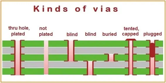
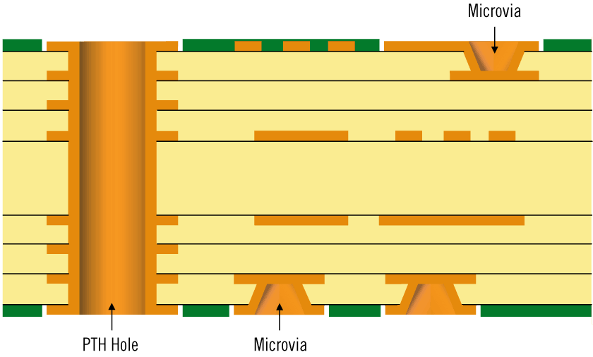
  • Blind Microvias: Connect an outer layer to one or more inner layers but do not extend through the entire board
  • Buried Microvias: Internal connections that do not reach any outer layer of the PCB
  • Stacked Microvias: Series of microvias placed directly on top of each other, connecting multiple layers
  • Staggered Microvias: Offset from each other rather than stacked directly, requiring fewer processing steps
  • Via-in-Pad: Microvias placed directly in component pads, allowing for higher routing density

Microvia Manufacturing Process

PCBsync utilizes state-of-the-art laser drilling technology to create precise microvias with consistent quality. Their process ensures reliable connections between layers, with proper copper deposition and, when necessary, copper filling for stacked microvias.

Technical Specifications

PCBsync’s HDI PCB manufacturing capabilities include:

  • Trace Width and Spacing: Down to 3 mils (approximately 75 micrometers)
  • Via Diameter: As small as 0.006 inches (approximately 150 micrometers)
  • Aspect Ratio: Maintains industry-standard recommendations of 6:1 to 8:1 for through-hole vias
  • Layer Count: Flexible configuration based on client requirements
  • Surface Finishes: HASL, Lead-free HASL, ENIG, Immersion Silver, Immersion Tin, OSP, Soft Wire Bondable Gold, and Hard Gold
  • Solder Mask Colors: Available in various colors, including Red, Green, Black, Blue, and White

Manufacturing Process Excellence

PCBsync’s HDI PCB manufacturing process incorporates several critical steps that ensure high-quality products:

  1. CAM Processing: Transforms design data into manufacturing data through Computer-Aided Manufacturing
  2. Core Fabrication: Creation of the standard inner layers of the PCB
  3. Sequential Build-Up: Addition of HDI layers through a series of lamination, drilling, and plating processes
  4. Copper Deposition: Controlled plating process to ensure an average of 25μm thickness through the holes, meeting IPC class 3 specifications
  5. Quality Control: Multiple inspection points throughout the manufacturing process

Quality Assurance

As an ISO9001 certified PCB assembly house, PCBsync operates under rigorous quality control procedures that ensure customer requirements are met at every stage of development. Their quality assurance system includes:

  • First article inspection before proceeding to full production
  • Open and short testing for all PCBs
  • Advanced inspection equipment including AOI Testing, 3D AOI Testing, 3D SPI Testing, X-ray inspection, and In-Circuit Testing
  • Strict supplier evaluation and yearly supplier assessment
  • Comprehensive customer service team for responsive communication

Applications of PCBsync’s HDI PCBs

PCBsync’s HDI PCBs are used in various applications that require high performance in compact form factors:

  • Smartphones and mobile devices
  • Wearable technology
  • Medical devices and equipment
  • Automotive electronics
  • Aerospace and defense systems
  • IoT devices
  • Consumer electronics
  • High-speed networking equipment

Benefits of PCBsync’s HDI PCBs

Choosing PCBsync for HDI PCB manufacturing offers several advantages:

  • Cost Efficiency: A 6-layer HDI circuit board can offer the same functionality as an 8-layer standard PCB, potentially reducing manufacturing costs
  • Enhanced Reliability: Microvias provide better stability and reliability compared to larger through-holes
  • Space Optimization: The use of blind, buried, and microvias decreases board space requirements
  • Signal Integrity: Shorter connection paths improve signal quality and reduce electromagnetic interference
  • Manufacturing Expertise: Years of experience in producing complex HDI designs ensures high-quality results

Conclusion

PCBsync Technology has established itself as a reliable provider of advanced HDI PCB manufacturing services, offering comprehensive capabilities from 1+N+1 to 4+N+4 stackups and any-layer HDI solutions. Their technical expertise, quality assurance systems, and commitment to customer satisfaction make them an excellent choice for companies requiring high-performance HDI PCBs for today’s compact electronic devices.

As the electronics industry continues to demand smaller, lighter, and more powerful devices, PCBsync’s HDI PCB manufacturing capabilities will remain at the forefront of enabling technological innovation. With continuous investment in advanced manufacturing processes and quality control, PCBsync is well-positioned to meet the future challenges of HDI PCB design and production.

Metal PCB Capability

Providing 1- 4 layer Aluminum Base, Copper Base, Iron base PCB Manufacturing service.


Metal PCB Capacity

Request Flex PCB manufacturing quotation, Pls send PCB files to Sales@PCBsync.com

ItemDescription
1.Layer1- 4 Layers
2.MaterialAluminum / Copper Based/Iron Base
ManufacturerXimai (China)  ; Bergquist (USA)
3.Final Thickness0.02″ – 0.18″ (0.5mm- 4.6mm) tg130° – tg170°
4.Surface TreatmentRegular Lead: HASL
Lead- free: Lead- free HASL, ENG Gold; OSP, Immersion silver
5.Max/Min Board SizeMin: 0.2″x0.2″  Max: 43.3″x19″
6.Min Trace width/Min Clearance

0.5oz: 4/4mil

1oz: 5/5mil

2oz: 5/7mil

3oz: 7/8mil

4oz: 10/10mil

7.Min Hole Ring

0.5oz: 4mil

1oz: 5mil

2oz: 7mil

3oz: 10mil

4oz: 16mil

8.Copper Thickness0.5oz- 4oz
9.Min Hole size and ToleranceMin hole: 30mil (Final Thickness 0.5mm- 2.0mm)
45mil (Final Thickness 2.0mm- 4.6mm)
Tolerance: PTH±4mil, NPTH±3mil
10.Thickness of Plating LayerHASL:
Copper Thickness: 20um- 35umTin: 5- 20um
Immersion Gold:
Nickel: 100u”- 200 u”Gold: 2u”- 4u”
Hard Gold Plating :
Nickel: 100u”- 200 u”Gold: 4u”- 8u”
Golden Finger:
Nickel: 100u”- 200 u”Gold: 5u”- 15u”
Immersion Silver: 6u”- 12u”
OSP: Film 8u”- 20u”
11.Solder Mask ColorGlossy: Green, Black, Red, Yellow, White, Purple, Blue
Matt: Green, Black
12.Solder Mask ResolutionSolder Mask Thickness:0.2mil- 1.6mil
Solder Dam:Green 4mil/Other Color 5mil
Solder Mask Hole Plug Diameter:10mil- 25mil
13.Silk Screen ColorWhite, Black
14.Silk Screen SizeMin Width: 5mil; Height: 24mil
15.Testing VoltageTesting Fixture: 50V- 300VFlying Probe: 30V- 250V
16.Profile

CNC Tol: ±5mil

V- CUT Tol: ±5mil

Slot Min: 40mil

Angel: 15°, 20°, 30°, 45°, 60°

17.Bow and Twist≤1%
18.Accept StandardIPC Class 2; IPC Class 3; ISO9000

you can know more about rigid-pcb-capacity,  Any flexible PCB manufacturing ,design question, send email to us.

SMT Capability

Long known as electronic manufacturing industry pioneers, we continue that reputation by offering full in-house PCB manufacturing and quickturn/small quantity assembly capabilities.

SMT Assembly Capabilities

Request Flex PCB manufacturing quotation, Pls send PCB files to Sales@PCBsync.com
SMT CAPACITY : 4 MILLION POINTS PER DAY,

ItemCapability
1Single and double sided SMT/PTHYes
2Large parts on both sides, BGA on both sidesYes
3Smallest Chips size0201
4Min BGA and Micro BGA pitch and ball counts0.008 in. (0.2mm) pitch, ball count greater than 1000
5Min Leaded parts pitch0.008 in. (0.2 mm)
6Max Parts size assembly by machine2.2 in. x 2.2 in. x 0.6 in.
7Assembly surface mount connectorsYes
8Odd form parts:
LED
Resistor and capacitor networks
Electrolytic capacitors
Variable resistors and capacitors (pots)
Sockets
Yes
9Wave solderingYes
10Max PCB size14.5 in. x 19.5 in.
11Min PCB Thickness0.02
12Fiducial MarksPreferred but not required
13PCB Finish:1.SMOBC/HASL
2.Electrolytic gold
3.Electroless gold
4.Electroless silver
5.Immersion gold
6.Immersion tin
7.OSP
14PCB ShapeAny
15Panelized PCB1.Tab routed
2.Breakaway tabs
3.V-Scored
4.Routed+ V scored
16Inspection1.X-ray analysis
2.Microscope to 20X
17Rework1.BGA removal and replacement station
2.SMT IR rework station
3.Thru-hole rework station
 

18. Min IC Pitch :0.2mm

19. solder paster printer:0.2mm

20.POP Manufacturing capability: POP *3F

SMT Capability

Request Flex PCB manufacturing quotation, Pls send PCB files to Sales@PCBsync.com

SMT Assembly Capabilities

Extensive and high-performance PCB equipment

The quality of a product is always determined by the quality of the tools. At PCBsync we have set a new benchmark when it comes to high-end Printed Circuit Board manufacturing equipment. Quality is given pre-eminence at our facility. Our PCB equipment conforms to high quality standards and is procured locally as well as internationally.

Detailed listing of PCB board equipment

To give you an idea of the PCB equipment used in our state-of-the-art factory, we have listed the specifications and photographs of some of our current equipment.

Quick turn PCB manufacturing line

To meet the ever-increasing demand for PCB prototyping we acquired a quick-turn PCB manufacturing line in 2005. As a Printed Circuit Board manufacturer that exceeds industry standards, we continue to delight our customers by providing outstanding Printed Circuit Board. Now for 2 layers we can ship the PCB in 12 hours, 4 layers in 48 hours, 6 layer pcb in 72 hours.

What machine is required for PCB Assembly?

Request Flex PCB manufacturing quotation, Pls send PCB files to Sales@PCBsync.com

SMT Assembly Capabilities

SMT Assembly Capacity

Introduction

Printed circuit board (PCB) assembly is the process of soldering electronic components to a PCB. This allows the creation of a functional electronic circuit. There are various machines and equipment used in PCB assembly to automate the production process. The main machines include soldering machines, inspection machines, material handling equipment, cleaning equipment and more.

Selecting the right PCB assembly equipment is crucial to achieving high productivity, quality and yield. The choice of machine depends on factors like:

  • Type of components to be soldered
  • Production volume
  • Required precision and accuracy
  • Budget

This article provides a comprehensive overview of the different types of machines used in PCB assembly and discusses their features, working principles, advantages and typical applications.

Soldering Machines

Soldering is the most important step in PCB assembly. It involves melting solder to create permanent joints between component leads and PCB pads. The main types of soldering machines are:

Wave Soldering Machine

A wave soldering machine passes the underside of the PCB over a wave of molten solder to simultaneously solder all solder pads and component leads. The key components are:

  • Solder pot – Contains molten solder alloy
  • Pump – Generates the solder wave
  • Preheating stage – Preheats the PCB to ensure proper soldering
  • Fluxer – Applies flux to PCB before soldering
  • Conveyor – Transports PCB through the machine

Wave soldering is ideal for soldering through-hole components on mass production PCBs. It allows high throughput up to thousands of boards per hour. However, it is not suitable for soldering surface mount devices (SMDs).

Reflow Soldering Oven

A reflow soldering oven uses heat to melt solder paste and form solder joints between SMDs and PCB pads. The oven has multiple heating zones with increasing temperatures to heat up the board. The stages are:

  • Preheating – Slowly heats up the board to evaporate solvents from solder paste
  • Reflow – Heats the board above the melting point of solder to form joint
  • Cooling – Cools the board down to solidify solder

For small volumes, reflow ovens with infrared heating are used. For mass production, convection ovens with forced air circulation provide faster heating. The peak temperature is around 217°C.

Reflow ovens allow excellent soldering quality and are ideal for SMD assembly. However, cycle times are longer compared to wave soldering.

Selective Soldering Machine

A selective soldering machine solders specific parts on the board using a miniature solder wave or solder fountain. It has a solder pot, pump, fluxer and conveyor. The key difference from wave soldering is:

  • Soldering head – A precision soldering nozzle that selectively applies solder only where needed.

Selective soldering provides flexibility to solder both through-hole and SMD components. It is ideal for manual rework or soldering heat-sensitive components after reflow.

Inspection Machines

Inspection of solder joints and checking for defects is vital in PCB assembly. Common inspection machines include:

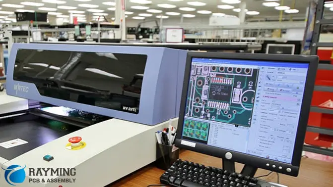
Automated Optical Inspection (AOI)

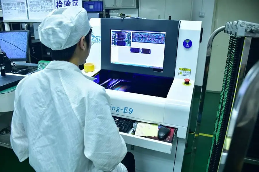
AOI machines use high resolution cameras to visually inspect the quality of solder joints. They use pattern recognition software to compare the PCB to a known good reference.

AOI provides fast and accurate inspection immediately after soldering. Both solder joints and component placement can be checked. However, it may not detect subtle flaws.

X-Ray Inspection

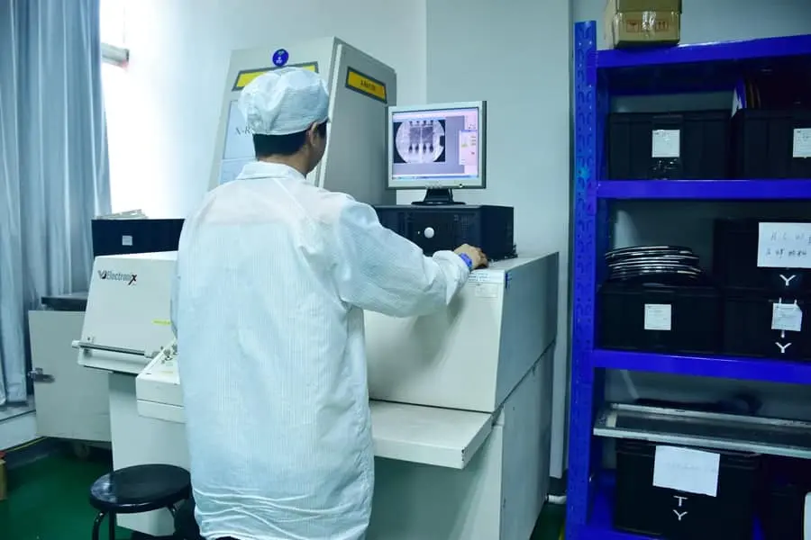
X-ray inspection uses X-ray imaging to see inside a PCB and inspect component soldering, placement and orientation. It creates a 3D image through the board, revealing hidden or buried defects.

X-ray inspection provides very detailed inspection. However, the equipment is more expensive than AOI. It is better suited for small boards.

Flying Probe Tester

This machine uses two movable “flying” probes to electrically test PCBs for shorts, opens, resistance and functionality. The probes move over the board and make contact with test points.

Flying probe testing verifies PCB assembly and detects manufacturing defects. It replaces fixture-based testing for small volumes.

Material Handling Equipment

Efficient material handling improves productivity in PCB assembly. Common material handling equipment includes:

Conveyor System

Conveyors are used to automatically transport PCBs between different assembly machines. This avoids manual material handling.

Automatic Solder Paste Printer

This machine uses stencils to apply the solder paste pattern onto the PCB before reflow soldering. It improves repeatability and reduces application defects.

Automatic Component Placer

This rapidly picks components from feeders and accurately places them on defined positions on the board. It avoids manual placement and improves quality.

Cleaning Equipment

After soldering, flux residue remains on the PCB which can be corrosive and conductive. Cleaning is essential. Common cleaning equipment:

Washers

Washers use liquids like deionized water to remove flux and other contaminants from the PCB surface. Different types include batch washers, inline washers, ultrasonic washers etc.

Cleaning Agents

Specialized cleaning agents like alcohols, solvents and detergents are used for effective PCB cleaning prior to washing.

Dryers

Dryers like centrifugal dryers are used to completely dry the PCB after washing to avoid any residual moisture.

Rework Equipment

Manual rework stations may be needed to repair defective boards or replace components. This allows recovery of PCBs instead of scrapping them. Common rework equipment includes:

Soldering & Desoldering Stations

Manual soldering/desoldering tools allow localised repair of solder joints without affecting the complete board. Hot air jets, infrared preheaters and vacuums ease the rework.

Fume Extraction Systems

Fume extractors remove harmful flux fumes released during rework soldering/desoldering. This improves operator safety.

ESD Control Equipment

Handling electronic components demands precautions against electrostatic discharge (ESD) which can damage sensitive devices. Common ESD control equipment:

Wrist Straps

Wrist straps ground the operator to safely discharge any static buildup.

ESD Mats

Conductive mats prevent electrostatic charge generation during handling and assembly.

Ionisers

Ionizers neutralize electrostatic charges by emitting positive and negative ions in the surroundings.

ESD Containers & Packaging

Components are stored and transported in static shielding bags and ESD certified containers.

Auxiliary Equipment

Some other auxiliary equipment required:

  • Storage racks for PCBs, components and materials
  • Workbench, chairs and tools for manual workstation
  • Solder wire, solder bars, fluxes, cleaning agents
  • Computer and software for production monitoring
  • Label printer for product identification
  • Measurement & testing equipment (microscopes etc.)
  • Fire extinguisher, first aid kit & PPE

Factors for Selecting PCB Assembly Equipment

The main factors guiding PCB assembly machine selection:

Throughput Rate

The production rate or number of boards that can be processed per hour. High throughput equipment like wave soldering and placement machines are needed for mass production.

Board Size

The dimensions of the PCBs being assembled. Large boards will need wider conveyors and large ovens.

Component Types

Through-hole, SMD or mixed? The component package types impact the soldering methods required.

Accuracy & Repeatability

Precision assembly demands machines with high accuracy, precision placement and consistent process control.

Multi-Product Versatility

Flexibility to switch between different PCB products, varying placement programs etc improves utilization.

Cost

Both equipment purchase cost and ongoing operating costs should be affordable.

Available Space

The floor space available in the production facility for accommodating the machines.

Operator Skill Level

Automated machines reduce dependency on operator skills. But rework still needs skilled operators.

Recommended Basic Setup

A basic setup for low volume PCB assembly could include:

  • Reflow oven for SMD soldering
  • Selective soldering machine for THD components
  • Automatic solder paste printer
  • Small component placement machine
  • AOI inspection system
  • Cleaning equipment like washer, dryer etc.
  • Rework station with microscope
  • Fume extraction system
  • ESD control equipment
  • Conveyor system for material handling

Whereas a setup for high volume manufacturing would include:

  • Wave soldering machine
  • Large reflow oven
  • High speed component placer
  • 2-3 AOI machines (pre-reflow and post-wave)
  • X-ray inspection system
  • Industrial washing systems
  • Automatic storage & retrieval systems
  • Extensive conveyor links between machines
  • Testing systems & flying probers

Main Suppliers of PCB Assembly Equipment

Some leading global suppliers of PCB assembly equipment include:

  • ASM – SMT placement, soldering and inspection systems
  • Juki – SMT assembling machines (placers, printers etc.)
  • Yamaha – Surface mount machines, bonders, printers
  • Panasonic – SMT production solutions
  • Europlacer – High speed, high precision component placers
  • Mycronic – Dispensing, jetting, placement and AOI
  • Nordson – Soldering (selective, wave) and dispensing systems
  • Vitronics Soltec – Wave and selective soldering machines
  • Asscon – Soldering machines (reflow, wave, selective)
  • Zymet – SMT screen printers, dispensers and placers
  • Manncorp – Reflow ovens,selective soldering and more
  • CTC – Conveyor systems for SMT production lines
  • Aqueous Technologies – PCB cleaning equipment
  • MPI – Automated optical inspection (AOI) machines
  • Viscom – 3D AOI and X-ray inspection systems
  • Takaya – Flying probe PCB test equipment
  • PACE – Manual soldering stations, fume extractors

Choosing suppliers with extensive experience, proven machine quality and responsive service support ensures long term equipment performance.

Conclusion

This covers the major types of PCB assembly machines and equipment currently used in the electronics manufacturing industry. The right set of machines with matching production volumes, PCB types, accuracy needs and budget ultimately enables efficient and quality PCB assembly. With numerous suppliers available globally, manufacturers can build an optimized production line meeting their exact requirements. By adopting more automation and smart manufacturing principles, PCB assembly facilities can reap benefits like higher throughput, improved quality, lower costs and greater reliability in electronic device production.

FAQs

What are the main steps in PCB assembly that require machines?

The four main processes in PCB assembly that use machines are:

  1. Solder paste printing
  2. Component placement
  3. Soldering (reflow or wave)
  4. Inspection by AOI/x-ray

Additional processes like flux application, cleaning, testing etc. may also use equipment.

What is the difference between pick and place and component placement machines?

Pick and place broadly refers to machines that pick components and place them on PCBs. However, in PCB assembly, component placement machine or SMT pick-and-place machine refers to the more sophisticated, high-speed, high-accuracy machines used.

How are large PCBs assembled if they cannot fit in SMT machines?

For large PCBs, manufacturers use modular SMT lines consisting of multiple smaller linked machines. Large PCB panels are divided into individual boards that pass through the machines separately before being panelized again. Conveyor systems link the machines.

When should AOI vs X-ray inspection be used in PCB assembly?

AOI provides a fast, low-cost inspection solution in most cases. X-ray inspection is more thorough in detecting hidden defects but costs much higher. X-ray is recommended for high reliability boards or periodically instead of inspecting every board.

What is the typical soldering temperature used?

For reflow soldering, the peak temperature is around 217°C depending on the solder alloy used. Wave soldering requires higher temperatures of 255-265°C for the solder to remain molten.

Prototype PCB Assembly House

PCBsync PCB Laboratory: Ensuring Quality Control in PCB Manufacturing

Request Flex PCB manufacturing quotation, Pls send PCB files to Sales@PCBsync.com

PCB Testing Laboratory High Quality PCB Products must be Tested by first-level PCB laboratory,PCBsync PCB not only 100% electronic testing , We also build high level Physics laboratory and The chemistry lab, We will deliver the PCBs beyond your expect.

Rayming’s Electronic Laboratory: Ensuring PCBA Assembly Quality

Request Flex PCB manufacturing quotation, Pls send PCB files to Sales@PCBsync.com

PCBSYNC has maintained a fully equipped Electronic Laboratory since 2017, dedicated to ensuring exceptional quality for all PCBA projects. Every circuit board assembly undergoes comprehensive testing in our facility before shipment to customers, guaranteeing reliability and performance.

For customers engaged in R&D projects, we extend access to our laboratory facilities to verify PCB designs. Our experienced engineers are available to provide technical assistance and testing support throughout your development process.

We conduct thorough verification including functional testing, environmental simulation, and reliability assessment to identify potential issues before they impact your product deployment. Our commitment to quality is reflected in our continuous investment in advanced testing equipment and expanding our capabilities to meet evolving industry requirements.

Partner with PCBSYNC for peace of mind knowing your electronic assemblies have been rigorously validated by our dedicated testing professionals using industry-leading equipment and methodologies.

Foundation of an Electronic Laboratory for PCBA Quality Assurance

Creating an effective electronic laboratory requires careful planning and implementation. The facility should feature anti-static flooring, controlled environmental conditions (temperature, humidity, and air quality), and sufficient lighting for detailed inspection work. The laboratory layout should follow the logical progression of the PCBA testing workflow, with dedicated zones for incoming component inspection, in-process testing, functional verification, reliability testing, and failure analysis.

This thoughtful organization minimizes cross-contamination risks while optimizing the efficiency of testing procedures. Additionally, the laboratory should include secure storage areas for reference boards, test fixtures, and documentation to maintain testing consistency over time.

Essential Equipment for Comprehensive PCBA Testing

Automated Optical Inspection (AOI) Systems

AOI systems use high-resolution cameras and sophisticated algorithms to detect visual defects such as missing components, incorrect polarity, misalignment, insufficient solder, or solder bridges. Modern AOI systems can capture 3D images to evaluate solder joint quality and component positioning with micrometer precision.

X-Ray Inspection Systems

X-ray inspection allows technicians to examine hidden solder joints beneath ball grid array (BGA) components, quad flat no-leads (QFN) packages, and other complex surface-mount devices. This non-destructive testing reveals voids, insufficient wetting, and internal structural defects that would otherwise remain undetected.

In-Circuit Test (ICT) Systems

ICT equipment uses a “bed of nails” fixture to make contact with test points on the PCBA, measuring electrical parameters and verifying component values against specified tolerances. This testing detects assembly errors, component failures, and manufacturing defects before functional testing begins.

Functional Test Equipment

Custom-designed functional testers simulate the operating conditions of the final product, verifying that the PCBA performs according to specifications. These systems can include power supply testing, signal generation, automated measurements, and software-driven test sequences that thoroughly exercise the circuit’s functionality.

Environmental Testing Chambers

PCBA reliability depends on performance across various environmental conditions. Temperature cycling chambers, humidity testing equipment, and vibration testing platforms subject assemblies to accelerated stress conditions, identifying potential weaknesses before they manifest in the field.

Solderability and Surface Analysis Tools

Specialized equipment for evaluating solder joint quality, surface cleanliness, and conformal coating integrity helps ensure long-term reliability. These tools can include dye penetrant testing apparatus, ionic contamination testers, and coating thickness measurement devices.

Failure Analysis Equipment

When defects occur, identifying root causes requires sophisticated analytical tools. Cross-sectioning equipment, scanning electron microscopes, thermal imaging cameras, and specialized probing stations enable technicians to isolate and characterize failure mechanisms at the component or board level.

Establishing Comprehensive Testing Protocols

A robust quality assurance system requires well-documented testing procedures that align with industry standards such as IPC-A-610 (Acceptability of Electronic Assemblies) and J-STD-001 (Requirements for Soldered Electrical and Electronic Assemblies).

These protocols should specify:

  • Sampling methodologies based on production volume and criticality
  • Detailed test sequences and procedures for each product type
  • Clear pass/fail criteria with measurable parameters
  • Documentation requirements and data retention policies
  • Handling procedures for non-conforming assemblies
  • Escalation pathways for recurring issues

Technical Expertise and Staff Development

The effectiveness of an electronic laboratory depends largely on the knowledge and skills of its personnel. Rayming should invest in:

  • Comprehensive training programs covering equipment operation, testing methodologies, and quality standards
  • Regular certification of testing technicians through industry-recognized programs
  • Cross-training to ensure operational flexibility and knowledge sharing
  • Continuing education to keep pace with evolving technologies and testing methods
  • Collaboration with engineering teams to improve both testing procedures and product designs

Data Collection and Statistical Process Control

Modern electronic laboratories implement sophisticated data management systems that capture testing results, track trends, and generate actionable insights. These systems enable:

  • Real-time monitoring of assembly quality metrics
  • Early detection of process drift before failures occur
  • Correlation analysis between defect types and specific production factors
  • Documentation for customer and regulatory requirements
  • Statistical process control implementation to maintain consistent quality

Integration with Production Processes

The electronic laboratory should not function in isolation but rather as an integral part of the manufacturing ecosystem. This integration requires:

  • Regular feedback loops between testing results and production processes
  • Collaborative problem-solving sessions involving laboratory technicians, process engineers, and production staff
  • Implementation of preventive and corrective actions based on testing data
  • Validation of process improvements through targeted testing
  • Development of new testing methodologies as product complexity evolves

Calibration and Measurement System Analysis

To ensure testing accuracy, all laboratory equipment must undergo regular calibration and validation. A comprehensive program should include:

  • Scheduled calibration against traceable standards
  • Gauge repeatability and reproducibility (GR&R) studies to validate measurement systems
  • Preventative maintenance schedules for all critical equipment
  • Validation of test fixtures against known reference assemblies
  • Documentation of all calibration activities and measurement system analyses

Customer-Specific Requirements Management

Different customers and industries often impose specialized testing requirements. The laboratory must remain adaptable to accommodate these variations while maintaining operational efficiency. This flexibility may necessitate:

  • Customer-specific test fixtures and procedures
  • Additional verification steps for critical applications
  • Enhanced documentation for regulated industries
  • Specialized reliability testing for harsh environment applications
  • Capability to implement new testing technologies as customer needs evolve

Conclusion

Establishing a comprehensive electronic laboratory represents a significant but essential investment for Rayming to ensure PCBA assembly quality. Beyond simply identifying defects, this facility serves as a central knowledge repository that drives continuous improvement throughout the manufacturing process.

By implementing advanced testing capabilities, rigorous protocols, and fostering collaboration between quality assurance and production teams, Rayming can differentiate itself in the competitive electronics manufacturing marketplace. As electronic products continue to increase in complexity and miniaturization, while reliability expectations remain stringent, a well-equipped electronic laboratory becomes increasingly critical to manufacturing success.

Through thoughtful planning, appropriate technology investment, thorough staff development, and seamless integration with broader manufacturing operations, Rayming’s electronic laboratory becomes not just a quality checkpoint but a strategic competitive advantage that delivers measurable value to customers through superior PCBA quality and reliability.

PCB PCBA Products

Technical

How is BOM cost calculated?

For PCB assembly, we require PCB design gerber format, drilling file and BOM. Click to download BOM template To avoid file missing, please include all files into one folder and compress it into .zip or .rar format.

Introduction

The bill of materials (BOM) is a critical component of manufacturing that lists all the parts and components needed to build a product. The total cost of the BOM determines the direct production costs for the product and has a large impact on the final pricing. Therefore, accurately calculating BOM costs is essential for manufacturers to understand profitability and make sound business decisions when bringing a product to market.

This article provides a comprehensive overview of how BOM cost is calculated for electronic and technical products. We’ll examine the factors involved in estimating the costs of material items, component pricing considerations, handling overhead expenses, and best practices for optimizing BOM cost analysis.

bill of material

What is a bill of materials (BOM)?

bill of materials is a structured list of all the parts and components that go into manufacturing a particular product. The BOM details the materials required to assemble each higher level component, subsystem, and ultimately the finished product itself.

For electronic products, the BOM encompasses:

  • Active components – Integrated circuits, transistors, diodes, LEDs, etc.
  • Passive components – Resistorscapacitors, inductors, transformers, etc.
  • Electromechanical parts – Connectors, switches, sensors, motors, etc.
  • PCBs – Bare printed circuit boards and assemblies.
  • Miscellaneous – Hardware, terminals, standoffs, fasteners, wiring, etc.

The BOM is much more than just a parts list. It also provides key information needed for costing analysis including:

  • Part numbers – Unique identifiers for each item
  • Descriptions – Details on the specific component
  • Quantities – How many of each item are required
  • Manufacturers – Vendor source for procuring each item
  • Unit pricing – Cost per item (a key input to total BOM costing)

Why BOM costing matters

Calculating an accurate BOM cost is critical for several reasons:

  • Determines production costs – The total BOM cost largely defines the direct manufacturing costs to build the product.
  • Enables accurate pricing – Pricing to distributors or end customers must cover total production costs plus margin. Undercosting the BOM results in losing money.
  • Aids sourcing decisions – Understanding material costs helps assess different supplier options during procurement and contracting.
  • Allows cost reduction – Detailed BOM analysis identifies opportunities to reduce costs through part substitution, design changes, different vendors, etc.
  • Supports cost tracking – BOM cost models provide the baseline for monitoring actual material costs as production ramps up.
  • Identifies cost risks – High cost items or uncertain estimates are visible for contingency planning or management attention.

In summary, solid BOM cost knowledge is required to make sound financial decisions as a product transitions from design to mass production. Both upfront accuracy and continuous cost management relies on robust BOM costing mechanisms.

BOM cost components

Several elements comprise the total cost calculated for a bill of materials. These include:

Component costs – The per unit prices for the raw materials, parts, and assemblies used to build the product. This constitutes the majority of the total BOM cost.

Labor costs – The labor expense (direct wages and benefits) required for assembly, soldering, insertion, finishing, testing, inspection, and other handling of components during production.

Tooling/fixture costs – Expenditures for production tooling like PCB assembly jigs, molds, or dies used to assemble or form parts of the product. These fixed costs are often amortized over the total production volume.

Allocation of overhead – A share of production overhead costs like facilities, utilities, management, quality, logistics, equipment maintenance, etc. is allocated to each product BOM based on its utilization of resources.

Margin – An additional markup percentage is added to cover non-production costs and ultimately provide profit margin. This markup structured depends on the company’s business model and cost management strategies.

The details of these cost elements will vary for different manufacturing environments, but together they comprise the full calculation of a product’s bill of materials cost.

Estimating component costs

The prices paid for the thousands of specific parts and materials that make up the BOM have the biggest influence on its total cost. Several techniques are used to estimate component costs:

Historical data – Costs paid in the past for the same or similar parts provides a good starting point estimate, adjusted for any known price trends.

Supplier quotes – Contacting component vendors and getting current price quotes on the required volumes delivers highly accurate estimates.

Industry data – Published electronic component price indexes and reports provide guidance on pricing trends for different commodities.

Parametric models – Cost models based on technical attributes like part type, tolerance, rating, and packaging can estimate costs when no direct data is available.

Design data – Information on required materials and processing can provide rough estimates based on market prices for those material stocks or processes.

Comparable analysis – Sometimes component pricing is estimated by comparison to another part of known price with similar attributes.

In most cases, a combination of these techniques produces the most reliable component cost estimates, cross-checked against multiple sources. Detailed quotes from vendors should be used to finalize pricing for volume forecasts.

Key variables in component pricing

BOM of PCB Assembly

Some of the key variables that affect the pricing of individual components include:

Component specifications – Higher temperature ratings, tighter tolerances, higher power capacities, etc. increase cost.

Materials used – Materials costs directly influence component costs, for example precious metals vs. commodity metals.

Packaging type – Surface mount vs. through-hole, trays vs. reels, etc. drive different costs.

Lead times – Components with short availability lead times often have premium prices.

Order volumes – Suppliers offer discounted pricing at higher order quantities due to lower per piece handling costs.

Market conditions – Component shortages, demand surges, commodity prices etc. impact market prices.

Geographic factors – Components sourced locally vs. overseas have different cost structures including import duties.

Company size – Large manufacturers get better pricing than smaller companies based on sheer order volume.

Lifecycle stage – End-of-life or obsolete components can have rapidly escalating prices as supplies diminish.

Careful consideration of these variables is necessary to develop accurate cost estimates, particularly for complex or custom components.

Handling overhead rates

SMT Bom checking

In addition to direct material costs, an allocated share of manufacturing overhead expenses is added to the BOM costs. This covers the infrastructure required to physically handle and process the materials into products.

Typical overhead costs charged to production include:

  • Facility costs – Rent, utilities, property tax, insurance, maintenance, etc.
  • Support labor – Supervisors, material handlers, quality inspectors, facilities staff, management
  • Depreciation – Equipment, tools, information systems
  • Supplies – Cleaning chemicals, lubricants, office items, small tools, etc.
  • Logistics – Warehousing costs, inbound/outbound transportation

To allocate these overhead costs, manufacturers calculate a handling rate per hour or per unit based on the capacity utilization by each product. Higher usage drives more overhead allocation. Rates are based on budgets and activity-based costing models.

Best practices for optimizing BOM costing

To achieve the most value from BOM costing analysis for making sound financial decisions, companies should follow these best practices:

  • Involve sourcing/procurement early – Work with the team responsible for purchasing and supplier contracting during initial BOM analysis to get realistic pricing.
  • Leverage design data – Work jointly with engineering teams to understand design factors that drive material selection and specifications to inform cost estimates.
  • Use standard component classifications – Assign standard material categories or grades to each component to aid in consistent cost rollups.
  • Perform risk analysis – Identify high cost components and items with uncertain or volatile pricing for management focus.
  • Link to ERP/MRP systems – Integrate BOM data with enterprise systems used for inventory, orders, and production planning to enable seamless cost analysis.
  • Regularly update for changes – Review component costs against quotes or market pricing continually throughout product lifecycles to maintain accuracy.
  • Analyze cost reduction opportunities – Dig into detailed BOM data to find areas for reduced material usage, alternate components, or lower cost suppliers.
  • Monitor and report actuals – Compare actual material costs booked during production to BOM forecasts to identify discrepancies and improve future estimates.
  • Use software tools – Modern platforms like Arena and FactoryLogix offer robust BOM cost management capabilities to eliminate spreadsheets.

By following these guidelines, organizations gain tremendous visibility into product cost structures and drivers. This allows smart decisions on pricing, sourcing, investments, and product direction to ultimately maximize profitability.

BOM Costing Case Study

Here is an example demonstrating real-world application of BOM costing analysis:

Acme Electronics was preparing to launch a new wireless security camera product for the consumer market. Engineering provided the BOM with 250 different components sourced from a mix of global suppliers.

The operations team imported the BOM data into the company’s cost management platform. Component costs were estimated using market price benchmarks and supplier quotes where available. Overhead rates were applied based on production line utilization.

The full analysis showed a total BOM cost of $42 per unit in 10k unit volumes. However the team identified two very high cost image processing ICs driving 15% of the total cost. A design change was approved to replace these with a lower cost standard part, dropping the BOM to $38.

This enabled Acme to reduce the retail price from $99 to $89 while maintaining margins. At an anticipated 100k unit volume over 2 years, the $11 reduction results in $1.1M additional profit. This demonstrates the power of detailed BOM analysis to impact the bottom line.

Conclusion

Performing robust and accurate bill of materials costing provides manufacturers critical insights into product profitability as they prepare to ramp from design into production. By following structured cost estimation approaches and continuous analysis best practices, companies make fully informed supply chain, pricing, and new product decisions.

Well managed BOM cost processes link design, procurement, finance, and operations functions to optimize production costs. As product complexities increase, capable BOM software tools deliver the modeling flexibility and rapid analysis required to maximize earnings in competitive markets. With proactive cost focus starting early in development, firms can accelerate new product introduction while ensuring each product delivers against financial targets.

FQA on BOM Costing

The Method of Creating Bill of Materials (BOM)

What are some warning signs of inaccurate BOM cost estimates?

Indicators of potential errors in BOM estimates include:

  • Component pricing outliers deviating widely from industry norms or experience
  • Excessive usage of “guesstimates” rather than actual data
  • Labor/overhead rates inconsistent with accounting records
  • Frequent large discrepancies between estimates and actual costs
  • Lack of supporting documentation for pricing assumptions
  • Minimal involvement from procurement/sourcing teams
  • Using old estimates without updating for current prices

What data sources provide the most accurate component pricing information?

The pricing data hierarchy from most to least accurate includes:

  • Direct supplier quotes based on required volumes
  • Recent purchasing history for the same components and volumes
  • Sourcing team market research and negotiated contracts
  • Published market pricing indexes validated by multiple sources
  • Parametric models based on technical attributes like materials, tolerances, packaging, etc.
  • Rough estimates by engineers based on specifications and materials

What are some common strategies used to reduce BOM costs?

Tactics to lower BOM costs include:

  • Consolidating designs to use fewer component variants
  • Negotiating lower component prices based on higher volumes
  • Substituting commodity grades for costly high-performance grades where possible
  • Choosing suppliers with lower cost structures
  • Adjusting designs to reduce quantity requirements through strategies like component sharing
  • Targeting high cost components for redesign or substitution
  • Identifying and eliminating unnecessary requirements driving overspecification
  • Value engineering reviews to simplify or streamline product architectures

What problems can inaccurate BOM costs cause during production?

Underestimating component prices leads to negative margins once in volume production. Overestimating BOM costs causes inflated pricing that can result in lost sales compared to the competition. Both outcomes lead to financial losses and potential product failures in the market.

How should BOM cost estimates be documented for future analysis?

BOM estimates should capture details like:

  • Reference sources for all component pricing like quotes, indexes, models, etc.
  • Assumptions on volumes ordered for each component
  • Allowances made for rises in future component prices
  • Basis for overhead rates applied and allocation methodology
  • Contingencies included for high risk or uncertain cost items
  • Descriptions of any product redesign iterations impacting the BOM

This documentation enables future review of the logic behind estimates.

sap bom tables

How to Convert PCB to Schematic Diagram?​

Converting a Schematic into a PCB Layout, or PCB to schematic diagram services 

PCB to Schematic Diagram

Esimate Cost converting PCB to shematic diagram, Pls send email to Sales@PCBsync.com Now

pcb schematic
PCB Schematic Diagram

Here are step by step introductions on how to convert PCB to schematic diagram and schematic diagram to PCB file.

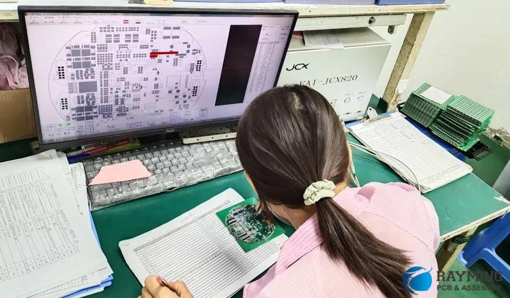
Step 1: The engineer analyzes the PCB layout through the circuit board and then divides the circuit into several units.

Step 2: Prepare two computers, one of which is used to view PCB documents, and the other is used to draw circuit diagrams.

Step 3: Retrieve the components in the unit circuit and do layout according to our work experience.

Step 4: Highlight the PCB document on the computer and then link it to another computer. After the link is completed, the network needs to be deleted.

Step 5: Repeat the first two steps until all files in the PCB document are deleted. After that, the engineer can optimize the schematic.

How to draw circuit diagrams according to real products?

When repairing electronic products, engineers often encounter problems finding the drawings, especially for legacy products;  the circuit diagrams may no longer exist. In this case, to analyze and improve the product, it is necessary to draw a circuit diagram based on the actual product. The skills of this operation are as follows:

1.Use the components with a large volume and many pins as a reference for drawing. Use this as a reference to start drawing, which can ensure accuracy andimprove work efficiency.

2. When an engineer is printing a circuit board, be sure to label the components and pay attention to the regularity of the serial number. They cannot randomize or remember which one to write. Write and arrange according to a particularorder and rules to ensure that it is not easy to make mistakes in the drawing process.

3. Without marking the serial number of the components, if the engineer wants to improve analysis and proofreading, you have to number the components yourself. It is not annoying;otherwise, the later work will be more difficult. Important components must be marked so that they will not be missed in the process of drawing the schematic.

4. Correctly distinguish the various wires on the circuit board. There are various wires on the circuit board,such as power wire, ground wire, signal wire, These wires have different layout positions, rules, and functions. When drawing a schematic, you must figure it out.

5. When drawing a sketch, be sure to use transparent tracing paper and mark it with colorful pens. It is convenient to identify, modify,and analyze the circuit to reduce errors. In addition, when drawing a circuit diagram, try to find a similar circuit diagram for reference so that there is a multiplier effect, which is very worthy of reference for newcomers.

It can be seen from the introduction that the process of converting a PCB to a schematic diagram is not difficult. Still, many novices lack experience or have not operated before, so they will find it challenging to convert PCB into schematics.

Protel+PCB Convert Into Schematic – Detailed Steps

Full raiders from Protel PCB to SCH

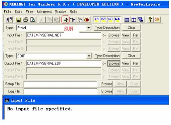
This article takes the 4 Port Serial Interface, provided by Protel 99Se, as an example. Open the PCB diagram, select the menu File-Export, export the Protel network table; the file name is abbreviated as Serial.Net. 2. Start the program Omninet for Windows, select Protel as the input file type (Type). In Input File 1, use Browse to specify the location of the netlist file. Select EDIF as the output file type (Type). In Output File 1, specify the file name and path of the output file. Then click Run (the running icon).

pcb to schematic

An output window pops up. Click Accept Data. Click “OK” when finished, and then click “Done” to close the output window. Exit Omninet for Windows.

circuit board diagrams

3.Start the E-Studio software and open the EDIF file generated in step 2

pcb diagrams
  1. Right-click the Serial.EDF file and select Generate Schematics:
pcb schematic design

The system pops up a window

circuit board schematic

Click OK.

5. Select menu File-Save As, and select ORCAD as the output format.Select Design v9.10 in the Save As drop-down menu.

altium schematic to pcb

Click Save to save. Click “OK” in the pop-up window to end.

The generated schematic can already be opened in ORCAD. The drawings are a bit big! The picture below is just its parts.

There is no hierarchy concept in drawings. No matter how complicated the circuit is, there is only one plane graph.

8 Ways to Restore PCB Schematic Diagram According to PCB Board

6. Convert ORCAD schematics into Protel schematics.

Because the output format of E-Studio does not have Protel, it must be converted separately. Protel 2004 is recommended for a better conversion effect.

Start DXP 2004, select menu File-Open, select Orcad Capture Design(*.DSN) for the file type.

kicad schematic to pcb

Click “Open.” An error occurred during the opening process, but the file conversion was successful. Click OK to close the error window.

altium designer schematic

Double-click 1.SchDoc, the file can be opened normally. The picture below is part of the file:

arduino pcb schematic

Select the menu File-Save AS, select Schematic Binary 4.0 (*.Sch). This is the format that 99Se can open.

easyeda schematic to pcb

At this point, the conversion of Protel 99Se PCB to the schematic diagram is complete.

It should be noted that this conversion may be useful for those with fewer components on the PCB. If there are many components on the PCB, the converted schematic diagram will be very large, and the network connection is extremely complicated. At this point, it is still difficult to interpret due to the lack of hierarchy or main thread. It is also not to be divided into multiple sub-graphs, and all networks are all connected.

In addition, the unconnected pins in the PCB no longer exist on the converted schematic. As shown in the example below:

schematic to pcb altium

Another disadvantage is that the footprint information of the component is gone and must be filled in again.

Although there is no footprint information, the network name is kept intact. After network comparison, no missing network is found.

A Basic Guideline from Schematic to PCB Design for Altium Designer

pcb to schematic

The electronic engineering industry is so vast and rapidly growing that technology is evolving day by day. There are currently numerous open-source software or Electronic Design Automation (EDA) or CAD software available to help designers design their electronic circuits and lay the PCB design along with tools available in the software to generate files that will be used directly by PCB fabrication house. 

Among these software, the most popular one is ALTIUM designer. The Altium Designer 18 will be discussed in this article. The Altium Designer gives you a complete platform where you can turn your imagination and ideas into reality.

We will discuss three main features of the Altium designer in the following sections: 1- Schematic Capture, 2- PCB layout, and 3- Fabrication Output Files.

Schematic Capture

The first step in turning the idea into reality is to do manual design or hand sketch on paper. This gives a clear understanding to the designer to know what he is looking for. Now the design on paper will be transferred to a CAD software like Altium. This process is called schematic capture. Having knowledge of the software, an expert will professionally capture the design in the schematic window.

File >> New >> Project >> PCB Project. Then right click on the project to “Add New to Project” >> Schematic

You can save your PCB project and schematic file with *.PrjPcb and *.sch extensions respectively. After saving, you can now start the placement of components from the library on the rightmost menu. You can add the manufacturer libraries available directly from the Altium website.

 Just download the library zip folder. Unzip it and copy-paste the folders inside C:\Users\Public\Documents\Altium\AD18\Library\ this folder. Now find the component in the library and place them on the schematic one by one. Ctrl+R will rotate the component. Press and hold the right click to “Pan,” and the Left Ctrl + Right-click will zoom in and out.

The top menu shows the wire, GND, library, place port, place text, move, drag, and select options.

The left panel shows the project files like schematic Diagram, PCB, Gerber, BOM, and other files are shown as sub-folder files inside the main project. Any changes made in the schematic will mark with a red symbol on the left panel schematic file. After you save changes, the red mark will disappear.

Now you interconnect the components using the wire or bus option. GND, VCC, and other signal ports can be placed accordingly. This will correspondingly generate “NETs.” The NET is the interconnection between two leads/legs of components. The net name shows the details of its connection. You can go to tools >> preference >> Schematics >> General, where you can edit and change the properties of the existing schematic sheet, like snap and visible grids. 

You can also annotate your components designators by Tools >> Annotation >> Annotate Schematics. You can change the sheet size by Right Panel Properties >>Page Options >> Formatting and Size >> Custom, and change the values of width and height according to needs, and change orientation to landscape or portrait. You can also switch between the units of measurement mm and mils.

The schematic capture is the basis of the PCB layout coming in the next step. Hence schematic capture should be completed free of errors. There should not be any error in the schematic design, and it must be cross-checked by another verification engineer to evaluate for any faults in the design. Otherwise, the wrong schematic will be translated into PCB and cause PCB not to function as expected.

PCB Layout

Now the next step is the PCB layout step. Right-click on Project panel >> Add new to Project >> PCB layout. A black color window will appear. This is the PCB layout documents where you will design the PCB layout. Now go to the schematic window and do the following:

Project >> Project options >> Class generation >> Uncheck generate rooms and uncheck electronic component classes. This is done to avoid any unwanted errors in PCB.

Now go to the schematic window. Design >> Update PCB Document. This will open the “Engineering Change Order” window. Now click on validate changes and then click execute changes. This will generate a green color tick sign on the right of the window. This shows everything is OK. Now go to the PCB document, and on the bottom right, your components will be available.

Drag and drop the components one by one onto the board. Now to reshape the board and go to View >> Board Planning Mode 1. You will see that the board color turns to green from black. Now go to Design >> Redefine Board Shape. Now the green color plus pointer will appear. You can now redefine the boundaries of your PCB board according to your needs. Remember to connect the last final edge with your starting edge/corner to complete the board shape. You can also use the edit board shape or modify board shape to change the board’s shape or style.

Now go to Design >> Rules. You can edit the PCB layout design constraints according to the PCB fabrication house capacity and limits and your design requirements. This is very important because while laying out PCB design (e.g., routing, placement of components, holes, vias, and other inner and outer layers), if there are violating constraints, the Altium will give you an error and will not proceed.

The main design rule constraints/clearances that need to be taken care of are track to track, track to SMD or THT pad, track to via, track to copper, SMD pad to SMD pad, SMD to THT pad, SMD pad to via, SMD pad to copper, THT pad to THT pad, THT pad to via, THT pad to copper, via to via, via to copper, and copper to copper clearances. Moreover, the maximum and minimum routing width and preferred values need to be defined. Solder masks and power planes with power pads constraints are also needed to be defined in design rules. Likewise, maximum and minimum via diameter and preferred values can be set in “Routing via Style.”

Now go to Design >> Layer Stackup Manager. This will show you the layer stack-up details, such as thickness, material, layer type, and name.

Now go to Route >> Auto Route >> All >> Route All. This will help you automatically route your components placed on the PCB according to the rules defined in the design rule wizard. The auto-routing will save ample time and effort but may not be a good choice when special care is needed for special ICs for EMI and other thermal considerations.

After everything is complete, go to Tools >> Design Rule Check (DRC). Running the DRC is important as it will identify any violations of design rules.

Fabrication Output Files:

Now that your PCB layout is done, it is time for Gerber and NC Drill File generation. These files are called PCB fabrication output files. Go to Files >> Fabrication Output >> Gerber Files. And NC Dill File. Select the appropriate unit and format for your Gerber and check to mark the “plot” of the corresponding layer you want to create Gerber. Keep all other parameters the same, and click OK.
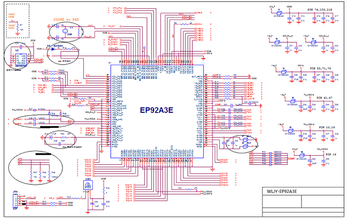
For NC (Numeric Controlled) Drill File, checkmark the “Generate Separate NC Drill Files for plated and non-plated through holes” and keep all other parameters the same and then click OK.

Convert Eagle Circuit Diagram to Altium Designer PCB Format

Now that open source hardware is prevalent, many open-source hardware manufacturers will make circuit diagrams public. For example, for Arduino, we can download the Arduino Eagle file on the official website. Still, many people don’t know the Eagle drawing software very well. So you need to convert the file into a format that can be opened with Altium Designer.

  1. Download the ULP file to be used on the official website of Eagle circuit diagram drawing software.
  2. Put the file in the ULP folder under the Eagle installation directory, as shown in the figure:
  1. pcb to schematic converter

from schematic to pcb

4. Click the ULP command in the command toolbar.

altium pcb from schematic

5.Select “export-protelpcb.ulp” in the directory of the pop-up dialog box and click to open.

reverse engineering pcb to schematic

6.Choose a suitable path and save the converted PCBfile.

altium from schematic to pcb

7.After clicking save, the following dialog box will pop up in the Eagle software, click OK.

schematic to pcb layout

8.At this point, the conversion of the PCB diagram has been completed. Double-click the saved file to open the file with Altium Designer, as shown in the figure:

pcb from schematic

8 Ways to Restore PCB Schematic Diagram According to PCB Board

When encountering some small objects, or encountering electronic products without drawings, you need to draw the circuit schematic according to the real thing.

There are the following points:

1. Select electronic components such as integrated circuits, transformers, transistors, etc., which are bulky, have many pins and play a major role in the circuit, and then draw from the selected reference pins to reduce errors.

2. If the component number (such as VD870, R330, C466, etc.) is marked on the PCB, since these serial numbers have specific rules, the components with the same Arabic numerals after the English alphabet are the same functional unit, so the drawing should be used. Correctly distinguishing the components of the same functional unit is the basis of the drawing pcb layout.

3. If the serial number of the component is not marked on the printed board, it is best to number the component yourself for easy analysis and proofreading. When designing printed circuit board components, the manufacturer generally arranges the components of the same functional unit relatively in order to minimize the copper foil routing. Once you find a device that has a core function, you can find other components of the same functional unit as long as you can find it.

4. Correctly distinguish the ground, power and signal lines of the printed board. Taking the power supply circuit as an example, the negative terminal of the rectifier connected to the secondary of the power transformer is the positive pole of the power supply, and a large-capacity filter capacitor is generally connected between the ground and the ground, and the capacitor casing has a polarity mark. 

The power and ground lines can also be found from the three-terminal regulator pins. When the factory is wiring the printed circuit board, in order to prevent self-excitation and anti-interference, the ground copper foil is generally set to the widest (high-frequency circuits often have large-area grounded copper foil), the power supply copper foil is second, and the signal copper is used. 

The foil is the narrowest. In addition, in electronic products with both analog and digital circuits, the printed boards often separate their ground lines to form an independent grounding grid, which can also be used as a basis for identification and judgment.

8 Ways to Restore PCB Schematic Diagram According to PCB Board

5. In order to avoid excessive wiring of the components, the wiring of the circuit diagram is cross-interleaved, resulting in a messy picture, and the power supply and ground lines can be used in a large number of terminal markings and grounding symbols. If there are many components, the unit circuits can be drawn separately and then combined.

6. When drawing a sketch, it is recommended to use transparent tracing paper, and use a multi-color pen to draw the ground wire, power cable, signal wire, components, etc. by color. When modifying, gradually deepen the color to make the drawing visually eye-catching for analysis of the circuit.

7. Proficiency in the basic composition of some unit circuits and classic drawing methods, such as rectifier bridges, voltage regulator circuits and op amps, digital integrated circuits. These unit circuits are directly drawn to form a frame of the circuit diagram, which can improve the drawing efficiency.

8. When drawing a circuit diagram, you should find a circuit diagram of a similar product as much as possible for reference, which will do more with less.

Blind Vias vs. Buried Vias: A Comparative Analysis for PCB design and Manufacturing

Vias serve as vital electrical interconnections between layers in a PCB stack-up. They create conductive pathways that allow components and traces to transmit signals across different board layers. Blind and buried vias enhance connectivity while minimizing the space required, making them particularly valuable in modern circuit design.

Various via types can be implemented in PCB manufacturing, each offering specific advantages for different design requirements. These specialized interconnections enable more complex and compact electronic designs by efficiently routing signals through the board’s structure.

Understanding Vias in PCB Design

PCB Vias
PCB Vias

Before we dive into the specifics of blind and buried vias, it’s essential to understand what vias are and their role in PCB design.

What are Vias?

Vias are small holes drilled through a PCB that are plated with conductive material. They serve as electrical pathways between different layers of a multi-layer PCB, allowing signals to travel vertically through the board. Vias are crucial for creating complex circuit designs in a compact space.

Types of Vias

There are three main types of vias used in PCB design:

  1. Through-hole vias
  2. Blind vias
  3. Buried vias

Each type has its unique characteristics and applications, which we’ll explore in detail throughout this article.

Read more about:

  • Via Covering
  • Via in Pad
  • Via filling
  • Annular Ring
  • Backdrill

Blind Vias: Connecting the Surface to Inner Layers

Blind vias are one of the advanced via types used in modern PCB design. Let’s examine their characteristics, advantages, and applications.

What are Blind Vias?

Blind vias are holes that connect an outer layer (top or bottom) of a PCB to one or more inner layers, but not to the opposite outer layer. They are called “blind” because they are visible from only one side of the board.

Characteristics of Blind Vias

  • Depth: Typically extend through 1-3 layers
  • Visibility: Visible from one side of the PCB
  • Diameter: Generally smaller than through-hole vias
  • Fabrication: Require specialized drilling and plating processes

Advantages of Blind Vias

  1. Space-saving: By not extending through the entire board, blind vias free up valuable real estate on inner and opposite outer layers.
  2. Improved signal integrity: Shorter signal paths reduce signal degradation and electromagnetic interference.
  3. Increased routing density: Allow for more traces on inner layers, enhancing design flexibility.
  4. Better RF performance: Shorter vias have less inductance, improving high-frequency signal transmission.

Applications of Blind Vias

Blind vias are particularly useful in:

  • High-density interconnect (HDI) boards
  • Mobile devices and wearables
  • RF and microwave circuits
  • High-speed digital designs

Buried Vias: Hidden Connections Between Inner Layers

Buried vias offer another approach to increasing PCB density and complexity. Let’s explore their unique features and uses.

What are Buried Vias?

Buried vias are holes that connect two or more inner layers of a PCB but do not extend to either outer layer. As the name suggests, they are completely “buried” within the board.

Characteristics of Buried Vias

  • Location: Entirely within inner layers of the PCB
  • Visibility: Not visible from the outside of the board
  • Fabrication: Require sequential lamination processes
  • Layer span: Can connect multiple inner layers

Advantages of Buried Vias

  1. Maximized surface area: Both outer layers remain free for component placement or routing.
  2. Enhanced signal integrity: Shorter signal paths and reduced crosstalk between layers.
  3. Improved reliability: Less exposed to environmental factors and mechanical stress.
  4. Design flexibility: Allow for complex interconnections between inner layers.

Applications of Buried Vias

Buried vias are commonly used in:

  • High-layer count PCBs
  • Aerospace and defense electronics
  • Medical devices
  • Advanced computing systems

Comparing Blind and Buried Vias

Now that we’ve examined both blind and buried vias individually, let’s compare them directly to understand their relative strengths and weaknesses.

Design Flexibility

Both blind and buried vias offer increased design flexibility compared to traditional through-hole vias. However, they differ in how they provide this flexibility:

  • Blind vias excel in connecting surface-mount components to inner layers, making them ideal for designs with numerous surface components.
  • Buried vias shine in creating complex interconnections between inner layers, benefiting designs with intricate internal routing requirements.

Space Utilization

When it comes to maximizing PCB real estate:

  • Blind vias free up space on inner layers and the opposite outer layer.
  • Buried vias leave both outer layers completely available for component placement or routing.

Fabrication Complexity

The manufacturing processes for both types of vias are more complex than those for through-hole vias:

  • Blind vias require precise depth control during drilling and special plating techniques.
  • Buried vias necessitate sequential lamination processes, which can increase manufacturing time and cost.

Signal Integrity

Both via types can improve signal integrity compared to through-hole vias:

  • Blind vias offer shorter paths for signals traveling from outer to inner layers.
  • Buried vias provide optimal paths for signals traveling between inner layers.

Cost Considerations

Generally, both blind and buried vias increase PCB manufacturing costs:

  • Blind vias typically have lower fabrication costs compared to buried vias but may still be significantly more expensive than through-hole vias.
  • Buried vias often incur higher costs due to the complex sequential lamination process required.

Implementing Blind and Buried Vias in PCB Design

blind holes pcb
buried hole pcb

Successfully incorporating blind and buried vias into your PCB design requires careful planning and consideration. Here are some key factors to keep in mind:

Design Rules and Constraints

When working with blind and buried vias, it’s crucial to adhere to specific design rules:

  • Aspect ratio: The ratio of via depth to diameter should typically not exceed 8:1 for reliable plating.
  • Layer pairing: Plan which layers will be connected by blind or buried vias early in the design process.
  • Via stacking: Consider stacking vias to connect multiple layers while minimizing the number of drill operations.

CAD Tool Considerations

Modern PCB design software typically supports blind and buried vias, but designers should:

  • Ensure their CAD tool can accurately represent and validate designs with these via types.
  • Use layer stack managers to define and manage complex layer structures.
  • Utilize design rule checks (DRC) specific to blind and buried vias.

Manufacturability Considerations

To ensure your design can be reliably manufactured:

  • Consult with your PCB fabricator early in the design process to understand their capabilities and limitations.
  • Consider the impact on yield and cost when deciding between blind and buried vias.
  • Be aware of minimum via sizes and maximum depths that can be reliably produced.

The Future of Blind and Buried Vias

As electronic devices continue to shrink while increasing in complexity, the use of blind and buried vias is likely to become more prevalent. Several trends and developments are shaping the future of these advanced via types:

Miniaturization

The ongoing drive towards smaller, more powerful devices will push the limits of via technology:

  • Expect to see even smaller diameter blind and buried vias.
  • Higher aspect ratios may become possible with advances in drilling and plating technologies.

Enhanced Materials

New PCB substrate and plating materials may improve the performance and reliability of blind and buried vias:

  • High-frequency laminates optimized for blind and buried vias in RF applications.
  • Advanced plating materials to improve conductivity and reliability in high-aspect-ratio vias.

Automation and AI in PCB Design

Artificial intelligence and machine learning are poised to revolutionize PCB design:

  • Automated via placement and optimization for blind and buried vias.
  • AI-driven design rule checking and signal integrity analysis.

3D Printed Electronics

As 3D printing technology advances, it may offer new possibilities for creating blind and buried vias:

  • Additive manufacturing of PCBs with integrated blind and buried vias.
  • Potential for more complex three-dimensional interconnect structures.

Conclusion: Choosing Between Blind and Buried Vias

The choice between blind vias, buried vias, or a combination of both depends on various factors specific to your PCB design requirements. Here are some key takeaways to guide your decision:

  • Use blind vias when you need to connect surface components to inner layers while maximizing inner layer space.
  • Opt for buried vias when you require complex inner layer connections and want to keep both outer layers free for components or routing.
  • Consider a combination of both types for maximum design flexibility in high-density, complex PCBs.
  • Always balance the benefits of these advanced via types against the increased manufacturing complexity and cost.

In conclusion, both blind vias and buried vias offer powerful solutions for increasing PCB density and performance. By understanding their characteristics, advantages, and applications, PCB designers can make informed decisions to create more efficient, compact, and high-performing electronic devices. As technology continues to advance, mastering the use of blind and buried vias will become increasingly important for staying at the forefront of electronic design.

PCB Quality Control

1. E-Test
2.A.O.I. – Test (Automated Optical Inspection)
3. X-ray (check registration accuracy for multilayers)
4. CCD – Camera Controlled Drilling
Verification of manufacturing tolerances
5. Impedance control

How Can We Guarantee the quality of Printed Circuit boards

To satisfy our customers we focus on producing PCB with top quality. We have implemented the ISO9001 and QS9000 quality system . The perfect quality assurance system and various inspection equipment help us to monitor the whole production process, assure stability of this process and high product quality, meanwhile, advanced instruments and technology methods have been introduced to attain sustained improvement.

There’s many advanced inspection and test instruments in PCBsync. which assures products”reliability of finished products.

This DRC check will check the netlist and layout against the PCB design constraints and rules. It checks the board’s component placement and trace routing integrity for overlapping components, untraced pins, incorrect layer placement and constraints that are WHERE set for trace width routing and clearances.We also do the manufacturing rule check to make sure the PCB design is manufacturable. If we find any errors we will get in contact with the customer.

Frist .DRC Check

The Design Rules Check (DRC) is a very important step in PCB quality control. When we receive a new PCB order from a customer, we will use an automated tool to verify that the layout does not have any specific placement, routing or other addressable layout errors.?

The 2nd. 100% Electrical Testing

Prototype Orders: We offer Flying-Probe E-Test for small volume and prototype orders. Your circuit board (PCB) is checked through a device called a Flying-Probe E-Tester. The Flying probe testers we use have few restrictions on access, require no test fixtures, and can test boards with virtually unlimited number of nets. The Tester will check for short circuits, open circuits and make sure the nets of the PCB we made is the same as the nets in your design. After testing is complete, the fail rate of your boards will be less than 1% ?

Production Orders: We use Testing fixtures to test production orders. A bed of nails tester is a traditional electronic test fixture which has numerous pins inserted into holes in an Epoxy phenolic glass cloth laminated sheet (G-10) which are aligned using tooling pins to make contact with test points on a printed circuit board.

The fixture contains an array of small, spring-loaded pogo pins; each pogo pin makes contact with one node in the circuitry of the DUT (device under test). By pressing the DUT down against the bed of nails, reliable contact can be quickly and simultaneously made with hundreds or even thousands of individual test points within the circuitry of the DUT.

The Tester will check for short circuits, open circuits, and make sure the nets of the PCB we made is the same as the nets in your design. After testing is complete, the fail rate of your boards will be less than 0.1% ?

AOI(Automated optical inspection)

We use an AOI to check the inner layers of multi-layers PCB. AOI visually scans the surface of the PCB. The board is lit by several light sources and observed by a scanner or by a number of high definition cameras. This enables the monitoring of all areas of the board.

AOI for a bare PCB board inspection will detect these features:

* Line width violations

* Spacing violations

* Excess copper

* Missing pads ? I.e. a feature that should be on the board is missing

* Shorts circuits

* Cut traces or pads

* Hole breakage.( Breakout ) ?I.e. a drilled hole (via) is outside of its landing pad?

This inspection is much more reliable and repeatable than manual visual inspection.

We are ISO 9001:2008 certified. And we briefly describe our quality control system as such:

* Our quality policy is a formal statement from our management, closely linked to our business and marketing plan and to our customer needs. Our quality policy is understood and followed at all levels and by all employees. Our employees will use measurable objectives to work towards.

* All Quality control data is recorded. Records will show how and where raw materials and products were processed, this allow products and possible problems to be traced to the source. Our quality control system is regularly audited and evaluated for conformance and effectiveness.

*Our quality control system records the customer requirements and creates a system for communicating with customers about product information, inquiries, contracts, orders, feedback and complaints.

* We regularly review performance of our quality control system through internal audits and meetings. We determine whether or not the quality system is working and what improvements can be made. We will deal with past problems and potential problems. Our system keeps records of these activities and the resulting decisions, and monitors their effectiveness.

* We documented the procedures for dealing with actual and potential non-conformances (problems involving suppliers or customers, or internal problems). Our system makes sure that all product(s) deemed “BAD” are quarantined and that no one can use the bad product until we can determine what to do with said bad product, We will seek and deal with the root cause of the problem(s) and keep records to use as a tool to improve our system.

The 4th . UL:E472163

Our products comply with UL safety certification 94V-0. Our UL number is E472163. All our PCBs meet a flame rating 94V-0 and satisfy all UL requirements. The flame rating per UL 94 defines a polymeric part ‘s resistance to fire. Typical ratings for PCB material are 94V-1 or better. The lower the number, the higher the flame rating (e.g., 94V-0 has a higher rating than 94V-1).

We are UL certified and our company logo can be traced back to UL ‘s authorized PCB manufacturers list. To be authorized in this category, a PCB manufacturer is subject to independent UL inspections of its manufacturing process and materials. You can check our UL documents at :  https://database.ul.com/cgi-bin/XYV/template/LISEXT/1FRAME/showpage.html?name=ZPMV2.E472163&ccnshorttitle=Wiring,+Printed+-+Component&objid=1084381836&cfgid=1073741824&version=versionless&parent_id=1073814637&sequence=1

RoHS

The Restriction of Hazardous Substances Directive or RoHS was adopted in February 2003 by the European Union. The RoHS directive took effect on July 1, 2006, and is required to be enforced and become law in each member state. This directive restricts the use of six hazardous materials in the manufacture of various types of electronic and electrical equipment.

From July 1st 2006 electrical and electronic equipment introduced onto the Europe market must not contain lead, mercury, cadmium, hexavalent chromium, nor the flame retardants polybromide biphenyl, or polybromide diphenyl ether.

All our lead free finishings: Lead free HAL, Immersion silver, ENIG and OSP all comply with the RoHS requirements.

PCBA Quality Control

PCBA QC techniques that may be performed during PCB assembly include: 1. Visual Inspections 2. X-ray Inspection 3.AOI Test 4. Electrical Testing,  Flying Probe E Test, Bed of Nails Test  5. ICT Test 6. FCT Test

PCB Assembly Quality Control System

PCB Assembly Quality Control

X-Ray Inspection for BGA Assembly

Our automated X-ray inspection systems are able to monitor a variety of aspects of a printed circuit board in assembly production. The inspection is done after the soldering process to monitor defects in soldering quality. Our equipment is able to”see” solder joints that are under packages such as BGAs, CSPs and FLIP chips WHERE the solder joints are hidden. 

This allows us to verify that the assembly is done right. The defects and other information detected by the inspection system can be quickly analyzed and the process altered to reduce the defects and improve the quality of the final products. In this way not only are actual faults detected, but the process can be altered to reduce the fault levels on the boards coming through. Use of this equipment allows us to ensure that the highest standards are maintained in our assembly.

PCB Assembly quality checklist

Components Quality control

To make sure the components to be used are good quality, there are several processes that we follow:

1. An overview of the visual electronic components inspection process includes:

* Packaging examined:

-Weighed and checked for damage

-Taping condition inspected-dented package etc.

-Original factory sealed vs. non-factory sealed

* Shipping documents verified

-Country of origin

-Purchase order and sales order numbers match

* Manufacturer P/N, quantity, date code verification, RoHS

* Moisture barrier protection verified (MSL)-vacuum sealed and humidity indicator with specification (HIC)

* Products and packaging (photographed and cataloged)

* Body marking inspection (faded markings, broken text, double print, ink stamps, etc.)

* Physical conditions inspection (lead bands, scratches, chipped edges, etc.)

* Any other visual irregularities found

Once our visual distribution inspection is completed, products are escalated to the next level-electronic components engineering distribution inspection for review.

2. Engineering Components Inspection

Our highly skilled and trained engineers receive the components for evaluation at a microscopic level to ensure consistency and quality. Any suspect parts or discrepancies that are discovered in the visual inspection process will either be verified or discounted by taking a product sampling of the material/parts.

The engineering electronic components distribution inspection process includes:

* Review visual inspection findings and notes

* Purchase and sales orders numbers verified

* Verification of labels (bar codes)

* Manufacturer’s logo and date log verification

* Moisture sensitivity level (MSL) and RoHS status

* Extensive marking permanency tests

* Review and comparison to manufacturer datasheet

* Additional photos taken and cataloged

* Solderibility Testing, the samples undergo an accelerated ‘aging ‘ process before being tested for solderibility, to take into consideration the natural aging effects of storage prior to board- mounting; In addition to the Engineering Components Inspection we have a higher level of inspection under the customer request.

3. By customer request, all components can pass a thorough final inspection in our Assembly facility.


Detectable defects list

Defect No.Defect DescriptionSelected Inspection Technology(s)Defect ClassAutomated Detection by final prototype
1Dry jointsAOISolderingNo
4BGA voidingX-raySolderingYes
5BGA bridgingX-raySolderingYes
6BGA tiltedX-raySolderingYes
7BGA missing ballsX-raySolderingYes
8BGA poor wettingX-raySolderingNot reliable detection
9BGA poor reflowX-raySolderingYes
10Leaded CC poor heel jointX-raySolderingNo
13Leaded CC lifted leadsAOISolderingNo
14SOT SOIC lead liftAOISolderingNot reliable detection
15Solder ballsAOISolderingYes
16PTH solder poor fillAOISolderingNo
17PTH poor lead wettingAOISolderingNo
18Heat plane delaminationSAM/Active thermographyBoardYes
19Plastic Encapsulated DelaminationSAM/Active thermographyComponentsYes
20Chip capacitor crackSAM/X-rayComponentsYes
21Missing componentAOIPlacementYes
22Tomb-stoningAOISolderingYes
23FlippedAOISoldering/PlacementYes
24TiltedAOIPlacementYes
25Solder shortPassive thermographySolderingYes

PCB X-Ray Inspection: How It Ensures Quality in Electronics Manufacturing

The X-ray inspection is part of the process control in our quality management system, Not only detect issues in SMT, but the analysis of an X-Ray image can help to determine the root cause of a given defect, such as insufficient solder paste, skewed part placement, or improper reflow soldering profile.

To guarantee the optimal performance of electronic devices, X-ray inspection is conducted on PCBs at every stage of the assembly process. Since various categories of circuit boards adhere to different inspection standards, X-ray inspection has become a widely utilized technique. It is particularly effective in identifying defects that are invisible to the naked eye, ensuring higher quality and reliability.

What is PCB X-ray Inspection?

X-RAY Test

Demystifying the Technology

PCB X-Ray Inspection is a non-destructive testing method that uses X-ray technology to examine the internal structures of printed circuit boards. This advanced technique allows manufacturers to peer inside complex PCBs without causing any damage, revealing hidden defects that might otherwise go unnoticed until product failure.

Beyond the Surface: X-Ray vs. Traditional Methods

While traditional inspection methods like optical and visual inspections are still valuable, they’re limited to surface-level examinations. PCB X-Ray Inspection takes quality control to the next level by providing:

  1. Internal visibility: X-rays penetrate through multiple layers of a PCB, exposing issues within the board itself.
  2. Higher accuracy: X-ray systems can detect microscopic defects that are invisible to the naked eye.
  3. Comprehensive analysis: From solder joint integrity to component placement, X-ray inspection covers a wide range of potential issues.

The Critical Role in Modern PCB Manufacturing

As PCBs evolve to accommodate more complex designs, X-ray inspection becomes increasingly vital. It’s particularly crucial for:

  • High-Density Interconnect (HDI) boards
  • Multilayer PCBs
  • Boards with Ball Grid Array (BGA) components
  • Miniaturized electronics with intricate internal structures

These advanced PCBs often have hidden solder joints, internal vias, and densely packed components that are impossible to inspect visually, making X-ray technology an essential quality assurance tool.

How Does PCB X-Ray Inspection Work?

The Science Behind the Scan

At its core, PCB X-Ray Inspection relies on the same principles that make medical X-rays possible. Here’s a simplified breakdown of the process:

  1. X-ray emission: A controlled beam of X-rays is directed at the PCB.
  2. Penetration: The X-rays pass through the various layers and components of the PCB.
  3. Absorption: Different materials absorb X-rays to varying degrees, creating contrast.
  4. Image creation: A detector on the opposite side of the PCB captures the resulting image, which shows the internal structure of the board.

The PCB X-Ray Inspection Process: Step by Step

  1. Sample preparation: The PCB is placed in the X-ray machine, often on a movable stage for precise positioning.
  2. Parameter setting: Technicians adjust settings like voltage, current, and exposure time to optimize image quality.
  3. Scanning: The X-ray beam moves across the PCB, capturing images from various angles.
  4. Image processing: Advanced software enhances the raw X-ray images for better clarity and analysis.
  5. Inspection: Trained operators or AI systems analyze the images to identify defects or irregularities.
  6. Reporting: Findings are documented, often with annotated images highlighting areas of concern.

Types of X-ray Inspections: 2D, 2.5D, and 3D CT

PCB X-Ray Inspection comes in several flavors, each with its own strengths:

  1. 2D X-ray Inspection:

    • Provides a flat, top-down view of the PCB.
    • Ideal for quick checks and identifying obvious issues like solder bridging.
    • Limited in its ability to show depth or layered defects.
  2. 2.5D X-ray Inspection:

    • Combines multiple 2D images taken at different angles.
    • Offers some depth perception and can reveal hidden solder joints.
    • Better for inspecting BGAs and other complex components.
  3. 3D CT (Computed Tomography) Inspection:

    • Creates a full 3D model of the PCB’s internal structure.
    • Allows for “virtual cross-sectioning” without damaging the board.
    • Provides the most comprehensive view but is also the most time-consuming and expensive option.

Key Benefits of PCB X-Ray Inspection

Implementing PCB X-Ray Inspection in the manufacturing process brings a host of advantages that contribute to higher quality products and more efficient operations.

1. Detection of Hidden Defects

X-ray inspection excels at uncovering issues that would otherwise remain invisible until product failure. These include:

  • Solder voids: Tiny air pockets within solder joints that can weaken connections.
  • Misalignments: Components that are slightly off-center or tilted.
  • Bridging: Unwanted connections between solder joints or traces.
  • Internal cracks or breaks in PCB layers.

2. Quality Assurance for Complex PCBs

As PCBs become more intricate, traditional inspection methods fall short. X-ray inspection provides:

  • Reliable inspection of multi-layer boards.
  • Accurate assessment of dense, high-component-count designs.
  • Validation of proper assembly for miniaturized components.

3. Minimized Risk of Product Failure

By catching defects early, X-ray inspection helps:

  • Prevent field failures that could damage a company’s reputation.
  • Reduce warranty claims and product recalls.
  • Ensure the safety and reliability of critical electronic systems.

4. Cost Savings Through Early Detection

While X-ray inspection systems represent an investment, they often pay for themselves by:

  • Reducing rework and scrap rates.
  • Catching issues before they compound into larger, more expensive problems.
  • Improving overall yield and production efficiency.

Read more about:

  • A.O.I.
  • Flying Probe Test
  • Functional Testing
  • 3D Solder Paste Inspection

Common Defects Identified by PCB X-Ray Inspection

X-ray inspection is particularly adept at identifying several types of PCB defects that can compromise performance and reliability.

Voiding in Solder Joints

Voids are small air pockets or gaps within solder joints. While some level of voiding is often acceptable, excessive voids can lead to:

  • Reduced thermal conductivity
  • Weakened mechanical strength
  • Potential points of failure under stress

X-ray inspection can quantify the percentage of voiding in each joint, allowing manufacturers to ensure they meet industry standards.

Open Circuits

Open circuits occur when there’s a break in the electrical path. X-ray inspection can reveal:

  • Lifted pads
  • Cracked solder joints
  • Incomplete connections in plated through-holes

These issues might not be visible from the surface but can cause intermittent or complete failure of the PCB.

Short Circuits

Short circuits happen when there’s an unintended connection between two points in a circuit. X-ray inspection helps identify:

  • Solder bridges between adjacent pads
  • Whiskers or stray conductive particles
  • Internal layer shorts in multilayer PCBs

Catching these defects early prevents potentially catastrophic failures down the line.

Component Misalignment

Proper component placement is crucial for PCB functionality. X-ray inspection can detect:

  • Shifted BGAs or other hidden-joint components
  • Tombstoning (where one end of a component lifts off the board)
  • Insufficient or excess solder in joints

These alignment issues can cause intermittent connections or complete component failure.

Internal Layer Defects

For multilayer PCBs, X-ray inspection is invaluable in identifying defects within the board itself:

  • Delamination between layers
  • Broken or misaligned internal traces
  • Voids or inclusions in the substrate material

Such internal defects are impossible to spot with visual inspection alone and can lead to long-term reliability issues if left unchecked.

Applications of PCB X-Ray Inspection Across Industries

SMT X RAY CHECKING

The versatility and effectiveness of PCB X-Ray Inspection make it an invaluable tool across various sectors where electronic reliability is paramount.

Aerospace and Defense

In an industry where failure is not an option, X-ray inspection ensures:

  • Compliance with stringent military and aerospace standards
  • Reliability of mission-critical systems
  • Detection of counterfeit components

Automotive Electronics

As vehicles become increasingly reliant on electronics, X-ray inspection helps:

  • Validate the integrity of safety-critical systems like airbag controllers
  • Ensure longevity of components exposed to harsh environments
  • Maintain quality in high-volume production of automotive PCBs

Consumer Electronics

In the competitive world of consumer devices, X-ray inspection contributes to:

  • Quality assurance for high-density mobile device PCBs
  • Improved reliability of wearable technology
  • Reduced failure rates in mass-produced electronics

Medical Devices

For medical equipment where lives are at stake, X-ray inspection provides:

  • Validation of life-supporting and monitoring devices
  • Compliance with strict regulatory requirements
  • Assurance of long-term reliability for implantable devices

Telecommunications

In the realm of global connectivity, X-ray inspection ensures:

  • Reliability of network infrastructure components
  • Quality control for high-frequency PCBs in 5G equipment
  • Integrity of densely packed, multi-layer boards in networking gear

Limitations of PCB X-Ray Inspection

While PCB X-Ray Inspection offers numerous benefits, it’s important to be aware of its limitations to use the technology effectively.

Cost Considerations

  • High initial investment for quality X-ray equipment
  • Ongoing costs for maintenance and calibration
  • Potential need for specialized facilities to house X-ray machines

Skill and Expertise Requirements

  • Trained operators needed to run equipment and interpret results
  • Continuous education required to keep up with advancing technology
  • Potential for misinterpretation of complex X-ray images

Equipment Size and Maintenance Needs

  • X-ray machines can be large, requiring dedicated space
  • Regular maintenance and safety checks are necessary
  • Potential downtime for repairs or upgrades can impact production

Choosing the Right PCB X-Ray Inspection Service

Selecting a PCB X-Ray Inspection provider is a crucial decision that can significantly impact your product quality and manufacturing efficiency.

Factors to Consider

  1. Machine Capabilities:

    • Resolution and magnification options
    • 2D, 2.5D, or 3D CT capabilities
    • Handling capacity for your PCB sizes and types
  2. Expertise and Experience:

    • Years in the industry
    • Familiarity with your specific type of PCBs
    • Certifications and qualifications of technicians
  3. Turnaround Time:

    • Ability to meet your production schedules
    • Capacity to handle your volume requirements
  4. Reporting and Analysis:

    • Depth and clarity of inspection reports
    • Integration with your quality management systems
    • Ability to provide actionable insights
  5. Customer Support:

    • Responsiveness to queries and concerns
    • Willingness to collaborate on solving issues
    • Flexibility in accommodating special requests

Questions to Ask Your Provider

  • What types of X-ray systems do you use, and how often are they calibrated?
  • Can you provide sample reports from previous inspections?
  • What standards and certifications does your facility adhere to?
  • How do you ensure the security and confidentiality of our designs?
  • What is your process for handling and communicating critical defects?
pcb x ray inspection

Future Trends in PCB X-Ray Inspection

The field of PCB X-Ray Inspection continues to evolve, with several exciting developments on the horizon.

Advances in AI-based Defect Detection

  • Machine learning algorithms improving accuracy and speed of defect identification
  • AI-assisted classification of defect types and severity
  • Potential for fully automated inspection processes

Integration with Automated Manufacturing Lines

  • Real-time X-ray inspection as part of Industry 4.0 smart factories
  • Immediate feedback loops for process adjustment and quality control
  • Integration with MES (Manufacturing Execution Systems) for comprehensive traceability

Technological Improvements

  • Higher resolution X-ray detectors for even more detailed imaging
  • Faster scanning capabilities to keep pace with high-volume production
  • More compact and affordable X-ray systems making the technology accessible to smaller manufacturers

Why RayPCB is Your Trusted Partner for PCB X-Ray Inspection

At RayPCB, we understand the critical role that X-ray inspection plays in ensuring the quality and reliability of your PCBs. Our state-of-the-art X-ray inspection capabilities are just one part of our comprehensive PCB manufacturing and quality assurance services.

Our X-ray Inspection Expertise

  • Advanced 2D, 2.5D, and 3D CT X-ray systems
  • Highly trained technicians with years of experience
  • Rigorous quality control processes aligned with industry standards

Customer Success Stories

Our clients across various industries have benefited from our meticulous X-ray inspection services:

  • Helped an aerospace client reduce field failures by 35% through early defect detection
  • Assisted a medical device manufacturer in achieving 100% pass rate for FDA inspections
  • Supported a consumer electronics brand in reducing warranty claims by identifying subtle BGA defects

Get in Touch

Ready to experience the RayPCB difference? Contact us today for a quote or to discuss how our X-ray inspection services can enhance your PCB quality assurance process.

Conclusion

PCB X-Ray Inspection has become an indispensable tool in the quest for electronic perfection. As we’ve explored, its ability to peer into the hidden layers of PCBs provides unparalleled insight into potential defects and quality issues. From ensuring the reliability of life-saving medical devices to guaranteeing the performance of your smartphone, X-ray inspection plays a crucial role in our increasingly electronic world.

By embracing this technology, manufacturers can:

  • Detect and address issues early in the production process
  • Improve overall product quality and reliability
  • Reduce costs associated with failures and recalls
  • Stay competitive in a market that demands ever-higher standards of excellence

As PCBs continue to evolve, becoming more complex and miniaturized, the importance of X-ray inspection will only grow. Forward-thinking companies are already integrating this technology into their quality assurance processes, reaping the benefits of improved yields, enhanced reliability, and stronger customer trust.

Don’t let hidden defects compromise your products’ integrity. Partner with RayPCB to leverage our cutting-edge X-ray inspection capabilities and ensure that your PCBs meet the highest standards of quality. Contact us today to learn how we can support your commitment to excellence in electronics manufacturing.

Frequently Asked Questions

  1. Q: How long does a typical PCB X-ray inspection take? A: The duration can vary depending on the complexity of the PCB and the type of inspection (2D, 2.5D, or 3D CT). A simple 2D scan might take just a few minutes, while a comprehensive 3D CT scan could take several hours.

  2. Q: Is X-ray inspection safe for the PCB components? A: Yes, PCB X-ray inspection is non-destructive and does not harm the electronic components or the board itself when performed correctly.

  3. Q: Can X-ray inspection detect all types of PCB defects? A: While X-ray inspection is highly effective, it’s not infallible. Some surface-level defects might be better detected by optical inspection. It’s often best to use X-ray inspection as part of a comprehensive quality control strategy.

  4. Q: How often should PCBs be X-ray inspected during production? A: This depends on your quality control needs and production volume. Some manufacturers inspect every board, while others use statistical sampling. Critical applications often require 100% inspection.

  5. Q: What’s the difference between X-ray inspection and CT scanning for PCBs? A: X-ray inspection typically refers to 2D or 2.5D imaging, while CT (Computed Tomography) scanning creates a full 3D model of the PCB’s internal structure, allowing for virtual “slicing” of the board in any plane.

What is an AOI test in SMT ?

Automated optical inspection is a key technique used in the manufacture and test of electronics board. AOI enables fast and accurate inspection of PCB PCBA and in particular PCB to ensure that the quality of product leaving the production line is high and the items are built correctly and without manufacturing faults

Bare PCB AOI Test

For Bare printed circuit boards, The AOI test verifies the finished conductor trace image for deviations from the Gerber data and finds errors that the E-Test may not discover, such as (for example) narrowed, but still unbroken conductor traces.

The AOI test is especially important for the following application areas:

1. High frequency
2. High power loads
3. High data transmission rates
4. Op-amps with high amplification factors and input resistances

The inner layers of multilayer PCB use AOI to scan before they are pressed together. This guarantees the high reliability of multilayer boards.

SMT AOI Test

SMT AOI

Automated optical inspection (AOI) is a key test method used in surface mount technology (SMT) printed circuit board (PCB) assembly to detect defects and ensure quality. This article provides an overview of AOI covering:

  • How AOI works
  • Defect types detected
  • 2D vs 3D AOI
  • Inspection process flow
  • AOI machine types
  • False call reduction
  • Limitations of AOI
  • AOI vs other test methods
  • Implementing AOI inspection

Understanding AOI technology and capabilities is important for quality management and process control in electronics manufacturing.

How AOI Works

Automated Optical Inspection (AOI)

AOI machines capture high resolution images of assemblies and use image processing software to compare against a “golden board” reference to identify defects.

Image Capture

  • Color or black/white cameras mounted above board
  • Angled lighting to detect height variations
  • Board conveyed under cameras for 100% coverage

Image Analysis

  • Software compares images against golden board
  • Image processing algorithms detect anomalies
  • Trainable defect detection and classification

Results

  • Defect location coordinates and size data
  • Images/video of detected flaws
  • Reports with failure statistics
  • Pass/fail outcome

Defect Types Detected by AOI

AOI inspection can identify a wide range of assembly-related defects:

Component Flaws

  • Missing parts
  • Wrong or misloaded parts
  • Shifted component position
  • Incorrect orientation
  • Tombstoned parts

Solder Joint Issues

  • Insufficient solder
  • Excessive solder
  • Solder balls/splatter
  • Solder bridging
  • Solder voiding

PCB Defects

  • Trace damage
  • Hole plugging
  • Foreign object debris
  • Etching or plating issues
  • Pad lifting

Marking Flaws

  • Missing silkscreen print
  • Misaligned or unclear legends
  • Barcode readability

2D vs 3D AOI

2D AOI

  • Lower cost inspection
  • Images from single angle
  • Limited height inspection
  • Can miss some defects

3D AOI

  • Constructs 3D model of board
  • Multi-angle image capture
  • Accurate height measurement
  • Detects more defect types
Types of Faults AOI can Inspect

AOI Inspection Process Flow

A typical AOI inspection sequence is:

1. Setup

  • Program inspection routine
  • Optimize lighting, cameras, focus
  • Load golden board reference

2. Verify Settings

  • Test sample boards to tune detection
  • Refine algorithms and thresholds
  • Confirm proper failure calls and none missed

3. Production Testing

  • Automatic board handling and scanning
  • Continuous operation with pass/fail indication
  • Process monitoring and trend analysis

4. Review Failures

  • Review failure images and coordinates
  • Reject boards with critical defects
  • Categorize faults by type and severity

5. Reporting and Analysis

  • Generate reports with failure rates
  • Identify failure patterns and trends
  • Perform root cause analysis
  • Implement corrective actions to reduce defects

Types of AOI Machines

There are different configurations of AOI equipment:

Inline AOI

  • Integrated into production line
  • Inspects boards right after SMT process
  • Fastest defect detection at source

Standalone AOI

  • Flexible off-line operation
  • Samples boards from line
  • Verifies process quality

Dual Lane AOI

  • Two independent inspection lanes
  • Double throughput capacity
  • Redundant capability

Mini AOI

  • Benchtop systems
  • Lower cost solution
  • Limited inspection area

Reducing False Calls


False calls where AOI reports a defect incorrectly reduce efficiency. Strategies to minimize false calls:

  • Optimize lighting, thresholds, algorithms
  • Enhance golden board with all acceptable variations
  • Mark acceptable design features as allowed
  • Train AOI system with representative samples
  • Perform regular maintenance and calibration
  • Tune detection based on inspection history
  • Review calls before rejecting boards

Limitations of AOI Technology

Despite advanced imaging technology, AOI has limitations including:

  • Low contrast defects can be missed
  • Confusion between components and markings
  • Shadowing underneath or behind components
  • False calls from irregular board features
  • Limited underfill inspection capability
  • Difficulty detecting subsurface defects

AOI vs Other SMT Inspection Methods

Compared to ICT

  • AOI finds assembly flaws vs electrical testing
  • More detailed defect and location data
  • Can be applied before electrical test

Compared to X-Ray

  • AOI is lower cost and faster
  • X-ray reveals subsurface defects missed by AOI
  • AOI has higher throughput for production

Compared to SPI

  • AOI checks assembly after reflow
  • SPI checks solder paste print before assembly

Implementing AOI Inspection

Key steps for utilizing AOI effectively:

  • Select right AOI technology based on needs
  • Program inspection routines carefully
  • Understand limitations to avoid over-reliance
  • Use AOI data for focused repair and root cause
  • Correlate AOI findings with other test methods
  • Continuously improve programs through feedback
  • Apply AOI inline for fastest defect detection
  • Implement as part of quality management system

Conclusion

Automated optical inspection is a critical quality control technique used throughout the SMT assembly process. This article provided an overview of how AOI works to detect surface defects on PCB assemblies. Understanding AOI capabilities as well as factors like false calls and limitations helps manufacturing engineers apply AOI optimally as part of a comprehensive quality strategy. Implemented effectively, AOI provides valuable inspection data to improve yields, reduce escapes and achieve consistent product quality.

Frequently Asked Questions

Here are some common questions about AOI testing for SMT:

Q: What types of defects can AOI detect?

AOI detects missing, shifted or wrong components, solder defects, PCB flaws, barcode issues and more. It finds assembly-related rather than electrical defects.

Q: Does AOI replace functional PCB testing?

No, AOI complements electrical and functional testing. AOI verifies component placement while circuit tests confirm electrical operation.

Q: Can AOI be used for BGA inspection?

Yes, AOI can reliably inspect BGA solder joints. 3D AOI provides accurate measurement of solder ball heights.

Q: What is the difference between inline and standalone AOI?

Inline AOI inspects boards directly on the assembly line while standalone AOI allows off-line sampling.

Q: Does AOI completely eliminate escapes and field failures?

AOI dramatically improves defect detection but cannot find all failure mechanisms like latent defects. Multiple test methods are still required.

What is FCT Test Meaning to PCB?

We provide functional circuit test services, and strongly request all PCBA board doing FCT test before delivery, Pls try to provide testing file, testing steps when you design or when you place an order. 

Introduction

FCT (Functional Circuit Test) is an important testing method used during the manufacturing process of printed circuit boards (PCBs). It involves testing the functionality of the circuits on the PCB to ensure there are no defects before the board moves to the next stage of production.

FCT testing provides key insights into the quality and reliability of the PCB design and its ability to function as intended. For electronics manufacturers, performing FCT testing properly is crucial for avoiding costly errors and producing high-quality boards that work correctly when assembled into finished products.

This article will provide a comprehensive overview of FCT testing for PCBs. We’ll look at what FCT testing is, why it’s needed, how testing fixtures are used, the types of defects it finds, and the implications of FCT results for PCB manufacturers.

What is FCT Testing?

fct test

FCT stands for functional circuit test. It is a method of testing unpopulated or bare printed circuit boards to verify the electrical connectivity and functionality of the circuits based on the intended design.

The key goals of FCT testing include:

  • Validate PCB fabrication: FCT testing checks for any manufacturing defects, errors or flaws in the PCB fabrication process that can lead to malfunctioning circuits. This verifies the PCB vendor correctly fabricated the boards according to specifications.
  • Catch assembly errors early: By testing boards before they are assembled and populated with components, FCT testing can identify any issues in the bare boards that would be harder to detect after assembly. Catching errors early prevents wasting time and money on assembling defective boards.
  • Ensure design integrity: FCT confirms that the circuits and connections implemented on the fabricated board match the intended PCB design files and schematics.
  • Check for shorts and opens: The testing detects any unintended electrical connections (shorts) or breaks in continuity (opens) in the circuits on the bare boards that could lead to field failures upon assembly.
  • Evaluate manufacturability: FCT results provide feedback on the manufacturability of the PCB design and highlight any areas that may need to be improved or corrected in the design.

In summary, FCT provides a vital quality control gate between PCB fabrication and assembly to verify the fabricated boards meet functionality and reliability requirements for further production.

Why is FCT Testing Important for PCBs?

FCT testing provides a number of important benefits that make it crucial for verifying quality and preventing problems in the PCB production process:

Early Detection of Flaws

FCT testing allows detection of shorts, opens, and other fabrication defects on the bare PCBs before components are soldered onto the boards. This enables issues to be identified and corrected at an early stage of production when fixes are simpler and less costly.

Avoid Wasting Time and Money

Assembling defective PCBs results in wasted expenditures on component materials and labor. FCT testing prevents such losses by screening out faulty boards before the expense of assembly. The ROI of performing FCT usually far exceeds the cost of implementing testing.

Ensure Reliability

If undetected shorts, opens or other flaws make it through assembly, the PCBs are much more likely to fail in the field. FCT testing improves reliability by catching these latent defects early when they are easier to correct.

Provides Design Feedback

FCT can reveal design-for-manufacturing issues that may be difficult to identify through design reviews. Test results give designers important feedback to improve the manufacturability of current and future boards.

Meets Quality Standards

FCT testing demonstrates the fabrication process is under control and meets specifications. This provides confidence in quality for the PCB manufacturer as well as customers. FCT is required for PCB suppliers to meet many industry quality standards.

In summary, performing thorough FCT testing is a best practice that reduces risk, improves quality, and prevents avoidable problems in the PCB fabrication and assembly process. The benefits of early defect detection and process feedback well justify the investment in proper FCT procedures.

FCT Testing Fixtures

To perform FCT on printed circuit boards, specialized testing fixtures are used to interface the bare PCBs with test systems that apply signals and measure the board’s electrical responses. FCT fixtures provide both mechanical handling of the boards and electrical connectivity to test points on the board circuits.

Key Elements of FCT Fixtures

FCT fixtures are custom designed for each PCB design to provide the following key functions:

  • Physical Board Holding – The fixture incorporates a frame or plates to securely hold the PCB in a defined orientation and position. This may include features like vacuum channels or clamps to maintain consistent contact.
  • Test Point Interfaces – Interconnect mechanisms like test probes, pogo pins, or edge connectors are integrated to make electrical contact with standard test points or pads on the PCB. Popular options include bed-of-nails and flying probe test fixtures.
  • Guarding for Safety – The fixtures provide shielding or insulation around the PCBs for protection from electrical hazards during testing. Ground planes and covers are commonly used.
  • Handling Ease – Fixtures are designed for quick loading and unloading of boards by operators or handling equipment like robots. This improves testing efficiency and throughput.
  • Durability – Test fixtures are built to withstand the rigors of repeated test cycles over thousands of board testing without failure. Materials like stainless steel are often employed.

FCT Fixture Types

fct fixture

There are two primary categories of fixtures used for FCT testing:

Bed-of-Nails Fixture

This type of fixture uses an array of spring-loaded “nails” or pins to contact test pads on the PCBs. It provides access to test points across the entire board area. The bed-of-nails approach can test digital circuits and simple analog circuits.

Flying Probe Fixture

Flying probe fixtures use movable test probes on precision robots to target specific test points on the PCB. This provides more versatility to reach points on complex board geometries. Flying probe can test digital and more complex analog circuits.

Hybrid fixtures combining both bed-of-nails and flying probes are also available. The type of FCT fixture selected depends on the PCB design, complexity, test access needs, and other considerations.

Defects and Faults Detected by FCT

FCT testing checks for a variety of circuit defects and faults that can occur in the PCB fabrication process. By applying test signals and measuring the output responses, issues like the following can be detected:

Open circuits – A break in the conductive path between points that should be connected according to the design schematics. Opens may be caused by gaps or thinning of copper traces, incomplete holes, or other fabrication flaws.

Short circuits – An unintended conductive bridge between two points not meant to be connected per the design schematics. Causes include copper smearing, unwanted solder, or drill errors like plating through a hole wall.

Value faults – When impedances like capacitances or resistances are out of tolerance from their designed value due to variations or flaws in fabricated components on the PCB.

Leakage – Unwanted current flows between circuits that should be isolated, indicating insulation resistance issues. Often caused by contaminants like moisture or residues on the PCB surface.

Intermittent faults – Defects that appear intermittently during testing, indicating marginal or unstable connections likely to cause reliability issues over time.

Circuit logic faults – Circuits failing functional tests due to problems with fabricated connections or components that prevent correct logic function per the design.

Crosstalk – Unexpected signal coupling between neighboring traces, vias, or components due to fabrication variations. Can cause interference and noise.

Impedance faults – Incorrect characteristic impedance of transmission lines like microstrips that can impair signal integrity at high frequencies.

In addition to identifying the type of defect, FCT testing also locates the physical position of faults on the PCBs for diagnosis and correction. Catching these issues early prevents improper board performance or failures once assembled and deployed.

When FCT testing reveals defects in a manufactured PCB, further analysis is required to determine the root cause so the underlying process errors can be corrected. Typical steps in FCT failure diagnosis include:

  • Repeat testing – Re-test the fault location to verify the failure is consistent and not an anomaly. Intermittent issues may require multiple repeated tests to isolate.
  • Correlate to design data – Compare the failure location and type to the PCB layout, schematics, bill of materials and other design files. Review the nominal circuit characteristics expected at the test nodes.
  • Visually inspect the PCB – Use optical inspection and tools like high-power microscopes to look for visible defects or damage at the failure location that may explain the issue.
  • Take electrical measurements – Use multimeters, time-domain reflectometers, or other tools to take further electrical readings like continuity, resistance, capacitance, and impedance around the fault.
  • Review process records – Examine PCB fabrication, handling, and test records for any anomalies that could be related to the failure like unusual measurements, tolerances exceeded, or equipment issues.
  • Reproduce with design experiments – Make deliberate modifications to the design data like adding shorts or opens and re-fabricate test boards to attempt reproducing and better characterize the failure mode observed.
  • Perform materials analysis – In some cases, use analytical techniques like scanning electron microscopy to inspect PCB materials like laminates or drill holes for flaws indicating process errors.

By correlating multiple data points from testing, inspection, design records, and materials analysis, the factors responsible for FCT failures can usually be effectively identified so that PCB fabrication processes can be adjusted to prevent similar defects going forward.

Implications of FCT Test Results

The outcomes and data gathered from FCT testing have important implications for PCB manufacturers in terms of quality control, process adjustments, and communication with customers:

  • Pass/Fail criteria – PCBs must meet predefined limits for acceptable defect rates in order to pass FCT. Failed boards are rejected or subject to rework if possible.
  • Process adjustments – Failures pointing to systematic fabrication process errors require correcting the processes to address root causes. Common process tweaks may involve lamination, drill, plating, etching, or handling steps.
  • Verification of fixes – Once a process is corrected, further FCT testing on new boards verifies the failures are eliminated before full production proceeds.
  • Design rule updates – If FCT reveals design-for-manufacturing issues, it provides feedback to update design rules and recommendations to improve manufacturability.
  • Reporting – FCT results and data metrics are compiled into reports that allow monitoring fab process capabilities over time as a key performance indicator (KPI).
  • Documentation – Detailed FCT failure documentation provides records that can be referenced during quality discussions with customers. Thorough reporting demonstrates quality vigilance.
  • Continuous improvement – By providing closed-loop feedback on defects and corrections, FCT testing enables continuous refinement of PCB fabrication processes and design rules toward higher reliability and yields.

In summary, properly leveraging the data from FCT testing helps PCB manufacturers achieve improved quality, process control, and customer confidence.

FCT Testing Case Study

Here is an example demonstrating the value of FCT testing:

A PCB fabrication shop had recently upgraded their lamination presses and processes. A new board design was fabricated on the new lamination lines and subjected to standard FCT testing. Initial results showed a 15% failure rate due to shorting between two critical control signals on the boards not seen previously.

Further diagnosis using optical inspection identified the shorts were caused by insufficient layer-to-layer alignment resulting in unintended connections between vias and traces on different layers. By examining process data, it was also found that lamination thickness had decreased on the new presses.

Armed with these failure analyses, the manufacturer adjusted the lamination processes to increase layer alignment tolerance and final thickness. Retesting of new boards on the corrected lines showed the shorting failures were eliminated. Without the early detection provided by FCT testing, these defective boards likely would have been assembled and failed functionality testing later or in the field. Catching the issue with FCT prevented many headaches and costs down the road.

This real-world example demonstrates the value of effective FCT testing and failure analysis to identify issues and drive process improvements.

FCT Testing Best Practices

  1. To gain the full benefits of FCT testing for quality and reliability, PCB manufacturers should follow these recommended best practices:

    • Implement FCT testing for all new PCB part numbers as a standard procedure before ramping to volume production. Do not rely only on first article inspection.
    • Maintain thorough documentation of FCT procedures, test fixtures, results data, and failure analyses. Keep organized records and databases.
    • Set clear pass/fail criteria for maximum defect rates. Failed boards should trigger required corrective actions before further production.
    • Closely integrate FCT failure analysis with design, fabrication, and quality engineering teams to enable rapid diagnosis and correction of process issues.
    • Continuously improve FCT test coverage, speed, and automation. Evaluate new fixture and testing technologies.
    • Leverage statistical process control methods to identify process trends and out-of-control conditions from FCT data over time.
    • Use FCT findings to frequently update PCB design rules and recommendations for continually improving manufacturability.
    • Provide open communication of FCT results and diagnostics with customers to demonstrate fabrication quality control vigilance.

    With the accelerating complexity of PCBs and fabrication processes, thorough FCT testing plays an increasingly vital role in quality management. Following best practices ensures PCB manufacturers maximize the returns from their investment in FCT.


FQA on FCT Testing

fct functional circuit test
  1. What are some key questions FCT testing helps answer?

    FCT testing provides answers to critical questions including:

    • Are there any shorts or opens on the bare boards indicating potential defects?
    • Do all tested nodes show the right connectivity to adjacent points per the design?
    • Are there any indications of impedance issues or propagation delays that could affect signal performance?
    • Do the circuits function correctly when stimulated with logic test patterns and clocks?
    • Are any power or ground networks skewed out of tolerance on impedance or resistance?
    • Do analog circuits like oscillators operate within expected frequency ranges?
    • Are there any signs of crosstalk or leakage between circuits that should be isolated?


  2. How is FCT testing integrated into the PCB fabrication workflow?

    FCT testing is performed after all fabrication processing is complete but before solder mask, silkscreen, or surface finishes are applied to the PCBs. This allows access to test points that may be blocked after these steps. FCT occurs before routing the boards on to assembly and provides a quality gate to avoid wasting further value-add on defective boards.


  3. How do you design FCT test fixtures and test points?

    FCT fixtures are designed based on CAD data for each unique PCB design. Test points are added to the PCB layout in unused areas, often on non-functional edges/corners. Testpoint locations are optimized to access key nodes while minimizing fixtures complexity. Strategies like daisy-chaining can minimize total test points. Both fixture and board designers collaborate to enable effective testing.


  4. What is the difference between “flying probe” and “bed of nails” FCT testing?

    Flying probe testers use movable probes to target individual test points. This provides more versatility for complex boards but lower throughput. Bed of nails uses an array of fixed pins to contact boards and enables higher throughput but only for simpler board geometries. Hybrid fixtures can leverage benefits of both approaches.


  5. How can you calculate the ROI for implementing FCT testing?

    The ROI justification factors the costs of testing (equipment, fixtures, labor) versus the defect risks detected multiplied by their associated costs (rework, scrap, field failures). As an example, catching even a 2% defect rate before assembly could save millions in avoiding wasted components and recalls. The more complex and critical the PCB application, the higher the ROI.

Conclusion

FCT testing provides PCB manufacturers with invaluable quality control and feedback by enabling early detection of fabrication defects before boards proceed to assembly. Rigorous FCT procedures and failure analysis prevents avoidable functionality issues or field failures and the significant costs associated with them.

By validating designs, catching flaws, and driving process improvements, FCT testing delivers large returns on investment and is considered essential for quality management of PCB production. As PCBs grow more complex, FCT helps ensure they function correctly when deployed in finished products. With careful fixture design, testing best practices, and diagnostic diligence, manufacturers can leverage FCT to deliver the highest reliability and yields.

What is the ICT test?

In-Circuit Test will ensure 100% quality pass, When design your board, Pls request electronic engineers to pre-design ICT, We will use diagram to make ICT fixture, and 100% testing before shipping

Introduction

ICT stands for In-Circuit Test. It is an electronic testing method used to verify the quality and integrity of circuit board assemblies. ICT testing detects defects like shorts, opens, missing components, wrong values, misplaced parts, and improper solder joints.

This article provides a comprehensive overview of ICT covering test basics, fixture types, program development, test coverage analysis, optimizing fault diagnosis, considerations for combining with functional test, and selecting ICT solutions suited for production volumes.

What is ICT Testing?

ict test

In-circuit testing refers to testing a populated printed circuit board to verify:

  • Electrical connections between components per the design netlist
  • Presence of correct component values at specified locations
  • Absence of manufacturing defects like shorts or opens
  • Overall assembly quality and workmanship

ICT leverages mechanical “bed-of-nails” test fixtures that make temporary electrical contact with test nodes across the board being tested. The connected tester then energizes various circuit paths and checks that corresponding nodes are properly excited.

Deviation from expected node levels pinpoints defects in assembly such as wrong components, missing parts, poor solder joints, short circuits or open circuits. By energizing multiple circuit nets, ICT can rapidly validate board assembly quality prior to functional testing.

Contact Sales & After-Sales Service

Contact & Quotation

  • Inquire: Call 0086-755-23203480, or reach out via the form below/your sales contact to discuss our design, manufacturing, and assembly capabilities.

  • Quote: Email your PCB files to Sales@pcbsync.com (Preferred for large files) or submit online. We will contact you promptly. Please ensure your email is correct.

Drag & Drop Files, Choose Files to Upload You can upload up to 3 files.

Notes:
For PCB fabrication, we require PCB design file in Gerber RS-274X format (most preferred), *.PCB/DDB (Protel, inform your program version) format or *.BRD (Eagle) format. For PCB assembly, we require PCB design file in above mentioned format, drilling file and BOM. Click to download BOM template To avoid file missing, please include all files into one folder and compress it into .zip or .rar format.