Inquire: Call 0086-755-23203480, or reach out via the form below/your sales contact to discuss our design, manufacturing, and assembly capabilities.
Quote: Email your PCB files to Sales@pcbsync.com (Preferred for large files) or submit online. We will contact you promptly. Please ensure your email is correct.
Notes: For PCB fabrication, we require PCB design file in Gerber RS-274X format (most preferred), *.PCB/DDB (Protel, inform your program version) format or *.BRD (Eagle) format. For PCB assembly, we require PCB design file in above mentioned format, drilling file and BOM. Click to download BOM template To avoid file missing, please include all files into one folder and compress it into .zip or .rar format.
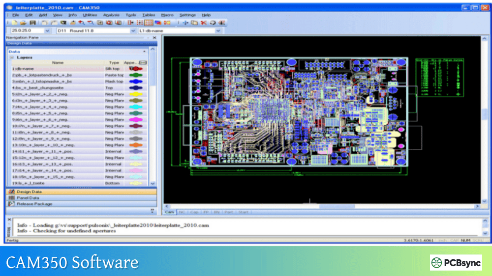
CAM350 for PCB Design & Manufacturing: Professional Workflow [2026]
Every PCB engineer knows that sinking feeling—you’ve spent weeks perfecting a design, exported your Gerber files, sent them to fabrication, and then received the dreaded call: “There’s a problem with your data.” In my experience processing hundreds of boards through manufacturing, CAM350 PCB verification has become the critical checkpoint that prevents exactly these scenarios.
This guide walks through the professional workflow for using CAM350 PCB tools in real production environments. Whether you’re a designer verifying output before release or a CAM engineer preparing data for fabrication, understanding this workflow eliminates costly delays and ensures your boards come back exactly as intended.
The transition from PCB design to physical board is where things go wrong. Errors in Gerber translation, mismatched apertures, connectivity issues that escape CAD-level DRC—these problems only surface during fabrication when they cost real money. CAM350 PCB verification catches these issues before they become expensive mistakes.
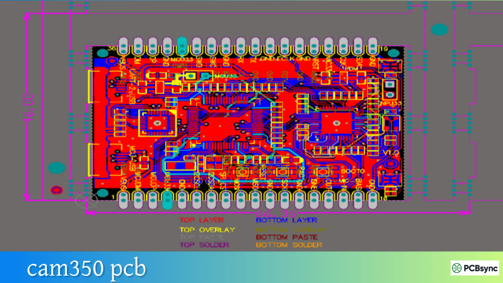
CAM350 serves multiple roles in the manufacturing chain: it’s a verification tool for designers, a production preparation system for fabricators, and a communication platform between both parties. The software handles everything from basic Gerber viewing through advanced DFM analysis, netlist comparison, panelization, and manufacturing output generation.
Key Benefits of CAM350 in PCB Production
Benefit
Impact on Production
Early error detection
Eliminates fabrication delays and re-spins
DFM analysis
Identifies manufacturability issues before tooling
After years of refining our process, I’ve developed a systematic CAM350 PCB workflow that catches problems consistently. Here’s the complete sequence from design handoff to manufacturing release.
Step 1: Data Import and Initial Validation
Start by importing your design data using File → Import → AutoImport. CAM350 handles multiple formats including Gerber (RS-274X and RS-274D), ODB++, IPC-2581, Excellon drill files, and DXF. For intelligent data formats like ODB++ or IPC-2581, you’ll retain component information, net connectivity, and layer stackup definitions automatically.
After import, perform immediate visual validation:
Check that all expected layers are present
Verify layer alignment by toggling visibility
Confirm drill data aligns with copper pads
Review board outline matches fabrication drawing
If layers appear misaligned, use Edit → Layers → Align to register them properly. Set your datum coordinate (Edit → Change → Origin → Datum Coordinate) to establish consistent reference points for all subsequent operations.
Step 2: Layer Organization and Stackup Definition
Proper layer typing is essential for accurate CAM350 PCB analysis. The software needs to understand which layers are signal, plane, soldermask, silkscreen, drill, and mill to perform intelligent checks.
Layer Type
Typical Extensions
Purpose
Signal
.GTL, .GBL, .G1-Gn
Copper routing layers
Negative Plane
.GP1, .GP2
Power and ground planes
Solder Mask
.GTS, .GBS
Mask openings
Silkscreen
.GTO, .GBO
Legend/marking
Paste
.GTP, .GBP
Stencil apertures
Drill
.DRL, .XLN
NC drill data
Board Outline
.GKO, .GM1
Mechanical boundary
Access the Layer Table (Tables → Layers or hotkey Y) to assign types and organize layer order. Proper stackup definition enables 3D visualization and supports blind/buried via analysis for complex multilayer boards.
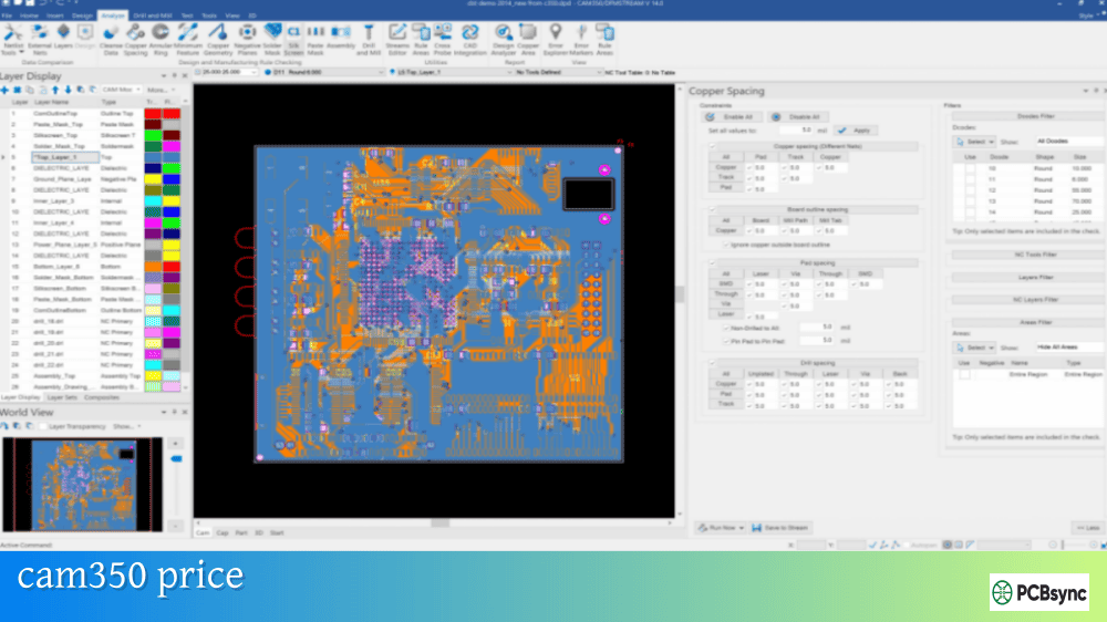
Step 3: Design Rule Check (DRC) Configuration
The DRC function in CAM350 PCB verification compares your design against specified manufacturing parameters. Configure checks based on your fabricator’s capabilities—these values vary significantly between standard and advanced processes.
DRC Parameter
Standard PCB
Advanced HDI
Minimum trace width
6 mil (0.15mm)
3 mil (0.075mm)
Minimum spacing
6 mil (0.15mm)
3 mil (0.075mm)
Annular ring
5 mil (0.125mm)
3 mil (0.075mm)
Drill to copper
10 mil (0.25mm)
6 mil (0.15mm)
Solder mask dam
4 mil (0.1mm)
3 mil (0.075mm)
Run DRC via Analysis → DRC and review all flagged violations. Some violations may be intentional design decisions—document these as accepted deviations rather than simply ignoring them.
Step 4: DFM Analysis for Manufacturability
DRC checks geometric rules, but Design for Manufacturing (DFM) analysis evaluates whether your board can actually be produced reliably. This is where CAM350 PCB analysis really earns its value.
DFM checks identify:
Acid Traps: Acute copper angles that trap etchant and cause incomplete etching. These create shorts or weak traces that fail under thermal stress.
Copper Slivers: Thin copper features prone to lifting during fabrication or thermal cycling. The tool flags traces and pours below minimum width thresholds.
Solder Bridges: Insufficient spacing between SMD pads where solder mask dams may not hold during reflow, causing shorts.
Thermal Relief Issues: Missing or inadequate thermal connections on plane layers that cause soldering problems during assembly.
Mask Slivers: Thin soldermask sections that won’t adhere properly and may flake off during assembly or use.
Run DFM analysis through Analysis → DFM Streams or the Streams Rule Check feature. Create reusable analysis profiles combining multiple checks into single execution sequences for consistent verification across projects.
Step 5: Netlist Comparison and Electrical Verification
Netlist comparison is the definitive test that your Gerber output matches your design intent. This catches errors that escape all other checks—accidental merging of nets, missing connections, opens from inadequate overlap, and shorts from unintended copper contact.
The CAM350 PCB netlist workflow:
Import reference netlist (IPC-D-356 format) from your CAD tool
Extract netlist from Gerber data using Tools → Netlist Extract
Run comparison via Analysis → Compare Netlists
Review results for opens, shorts, missing nets, and extra nets
This step has saved my projects more times than I can count. Translation errors, operator mistakes in Gerber generation, and accidental inclusion of non-electrical items in output files all show up here. Never skip netlist comparison—it’s your final electrical verification before committing to fabrication.
Step 6: Drill and Mill File Optimization
NC data requires verification and often optimization for manufacturing. Use the NC Editor functions to review and modify drill and mill data.
Key drill checks in CAM350 PCB preparation:
Minimum hole size meets process capability
Hole-to-hole spacing adequate for drill registration
Aspect ratios within fabricator limits
Slot dimensions and routing clearances verified
Tool table consolidated for efficient drilling
If drill files weren’t provided with the design package, CAM350 can create drill data from Gerber using Utilities → Gerber to Drill. First convert pad apertures to flash format, then extract drill hits from the flash locations.
For routing, verify that mill paths are closed contours with proper tool compensation. Check tab placement for depanelization and confirm clearances to copper features meet requirements.
Step 7: Panelization for Production
Single boards rarely go to fabrication—production panels maximize material utilization and enable efficient handling through the manufacturing line. CAM350’s panel functions streamline this process significantly.
Two approaches exist for CAM350 PCB panelization:
Merge Method: Load individual CAM350 databases as merged objects, arrange using Edit commands, then explode and consolidate layers. Best for combining different board designs into a single panel.
Panel Editor: Use the dedicated panel workspace with automated step-and-repeat, rail generation, tooling hole placement, and fiducial insertion. Choose the automated wizard or configure parameters manually for full control.
Panel Element
Purpose
Typical Specification
V-Score Lines
Depanelization
0.4mm remaining material
Mouse Bites
Tab routing
0.5mm holes, 0.8mm spacing
Tooling Holes
Fixture alignment
3.2mm diameter, ±0.05mm
Fiducials
Pick-and-place reference
1mm diameter, 3mm clearance
Rails
Handler clearance
5-10mm width
Step 8: Manufacturing Output Generation
With all verification complete and panelization finalized, export manufacturing data through File → Export. Generate separate outputs for:
Gerber files (RS-274X format recommended)
NC drill data (Excellon format, verify leading/trailing zero suppression)
NC mill/route data
IPC-D-356 netlist for bare board test
Centroid/placement data for assembly
BOM and assembly drawings
Always verify exported files by re-importing them into a fresh CAM350 session. This catches export configuration errors and confirms the data fabricators will receive matches your verified database.
Modern CAM350 PCB verification integrates bidirectionally with major CAD platforms. CrossProbing creates live links between CAM350 and tools like Cadence Allegro, OrCAD PCB Designer, and Siemens Xpedition.
With CrossProbing active, selecting elements in your CAD tool highlights corresponding features in CAM350, and vice versa. After DFM analysis identifies violations, use CrossProbing to jump directly to error locations in your design tool for correction. This dramatically accelerates the fix-verify cycle compared to manual coordinate lookup.
Automation Through Macros and Scripting
For production environments processing multiple boards daily, CAM350 PCB automation capabilities become essential. The built-in macro system records command sequences that can be replayed on subsequent designs, ensuring consistent processing across your entire workflow.
The VB Script API extends automation further, enabling:
Custom dialog interfaces for operator input
Conditional processing based on design characteristics
Automated report generation in custom formats
Integration with external systems and databases
Batch processing of multiple designs
Engineers who invest time in developing macros report processing time reductions of 50-70% for routine verification tasks. Start by recording your standard verification sequence, then refine the macro to handle edge cases and add error checking.
Best Practices for CAM350 PCB Production Workflows
Experience teaches hard lessons about what works in production CAM350 PCB workflows. Here are practices that consistently deliver results:
Always verify against original CAD data when available. Gerber files lose intelligence present in native CAD formats. When ODB++ or IPC-2581 output is available, use it—the additional information enables more thorough verification and easier troubleshooting.
Document deviations explicitly. When you accept a DRC violation as intentional (controlled impedance structures often trigger spacing warnings, for example), document the decision. Future engineers reviewing the project need to understand why violations were accepted.
Maintain configuration standards. Create templates for DRC parameters, DFM rules, and export settings matched to your primary fabricators. Consistent configuration prevents errors from mismatched settings between projects.
Verify exported data by re-importing. The few minutes spent loading exported files into a fresh CAM350 session catches configuration errors before they reach fabrication. This simple step prevents surprisingly common export-related problems.
Archive complete verification packages. Save the CAM350 database, verification reports, and accepted deviation documentation together. When questions arise during fabrication or assembly, having complete records accelerates resolution.
Common CAM350 PCB Troubleshooting Scenarios
Even experienced engineers encounter issues during CAM350 PCB processing. Here’s a quick reference for resolving the most common problems:
What file formats does CAM350 support for PCB data?
CAM350 PCB tools support comprehensive format coverage. Import formats include Gerber (RS-274D, RS-274X, Fire9000, Barco DPF), NC Drill/Mill (Excellon, Sieb & Meyer), IPC netlists (IPC-D-356, IPC-D-356A), ODB++, IPC-2581, DXF, GenCAD, and HPGL. Export formats include Gerber, NC Drill, ODB++, IPC-2581, DXF, and CAD formats like PADS ASCII and GenCAD depending on your configuration level.
How does CAM350 PCB verification differ from CAD-level DRC?
CAD-level DRC checks your design against rules within the design environment. CAM350 PCB verification checks the actual manufacturing output—the Gerber files, drill data, and production formats that fabricators will use. This catches translation errors, export problems, and issues that only manifest in the output data. Additionally, CAM350 performs DFM analysis that evaluates manufacturability against real fabrication capabilities, not just geometric rules.
Can CAM350 create drill files if the designer didn’t provide them?
Yes. CAM350 can generate drill data from Gerber files using the Gerber to Drill conversion. First convert drawn pads to flash format (Utilities → Draw to Flash), then extract drill hits from flash locations (Utilities → Gerber to Drill). The tool creates an NC drill file matching the pad aperture sizes. However, this method requires careful verification—always confirm the generated drill data against design documentation.
What’s the difference between DRC and DFM analysis in CAM350?
DRC (Design Rule Check) verifies geometric rules—minimum trace width, spacing, annular ring, etc. It confirms your design meets specified dimensional requirements. DFM (Design for Manufacturing) analysis evaluates whether the design can be reliably manufactured. DFM checks for acid traps, copper slivers, solder bridges, thermal relief issues, and other fabrication-specific concerns that may cause yield problems even when basic geometric rules pass.
Is CAM350 necessary if my fabricator performs incoming inspection?
While fabricators do perform CAM review, relying solely on their inspection creates delays and potential miscommunication. Your fabricator’s CAM engineer may interpret ambiguous features differently than you intended, or flag issues requiring design changes after you’ve committed to production schedules. Using CAM350 PCB verification before release ensures you catch and resolve issues on your timeline, with full understanding of design intent. Many engineers report that pre-release verification eliminates 90% of fabricator queries and significantly reduces turn-around time.
Conclusion
Implementing a systematic CAM350 PCB verification workflow transforms the design-to-manufacturing transition from a source of anxiety into a predictable, controlled process. The investment in proper verification pays dividends through eliminated re-spins, faster fabrication cycles, and boards that work correctly the first time.
The workflow outlined here—import validation, layer organization, DRC, DFM analysis, netlist comparison, drill optimization, panelization, and verified output generation—represents industry best practice developed through countless production cycles. Whether you’re processing your first board or your thousandth, this systematic approach ensures consistent, reliable results.
Start with the basics: import, verify alignment, run DRC, compare netlists. As you gain experience, incorporate DFM analysis, CrossProbing integration, and automated workflows through macros. The learning curve is manageable, and the return on investment is immediate—your first prevented fabrication delay will more than justify the effort.
Inquire: Call 0086-755-23203480, or reach out via the form below/your sales contact to discuss our design, manufacturing, and assembly capabilities.
Quote: Email your PCB files to Sales@pcbsync.com (Preferred for large files) or submit online. We will contact you promptly. Please ensure your email is correct.
Notes: For PCB fabrication, we require PCB design file in Gerber RS-274X format (most preferred), *.PCB/DDB (Protel, inform your program version) format or *.BRD (Eagle) format. For PCB assembly, we require PCB design file in above mentioned format, drilling file and BOM. Click to download BOM template To avoid file missing, please include all files into one folder and compress it into .zip or .rar format.


