Inquire: Call 0086-755-23203480, or reach out via the form below/your sales contact to discuss our design, manufacturing, and assembly capabilities.
Quote: Email your PCB files to Sales@pcbsync.com (Preferred for large files) or submit online. We will contact you promptly. Please ensure your email is correct.
Notes: For PCB fabrication, we require PCB design file in Gerber RS-274X format (most preferred), *.PCB/DDB (Protel, inform your program version) format or *.BRD (Eagle) format. For PCB assembly, we require PCB design file in above mentioned format, drilling file and BOM. Click to download BOM template To avoid file missing, please include all files into one folder and compress it into .zip or .rar format.
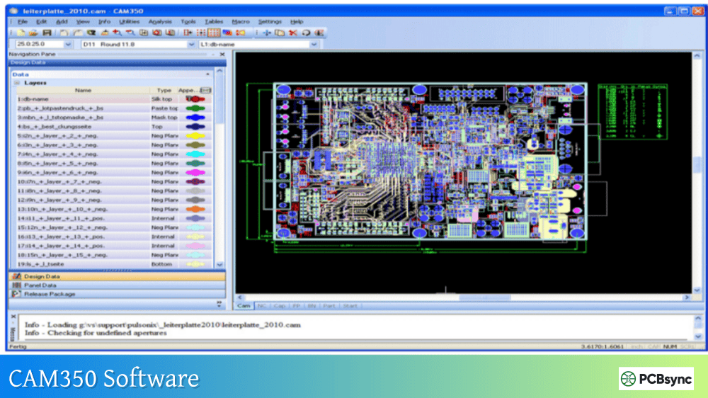
How to Use CAM350 with Gerber Files: Step-by-Step Tutorial [2026]
Working with CAM350 Gerber files is something I do almost daily as a PCB engineer, and I’ve learned that proper CAM processing can mean the difference between a smooth production run and costly fabrication delays. Whether you’re verifying design output before sending to a fab house or preparing manufacturing files as a CAM engineer, understanding how to use Gerber CAM350 workflows is essential knowledge.
This comprehensive tutorial walks through the complete process of importing, verifying, editing, and exporting Gerber files in CAM350. I’ll share practical tips that come from real production experience, covering everything from basic import procedures to advanced DFM analysis techniques.
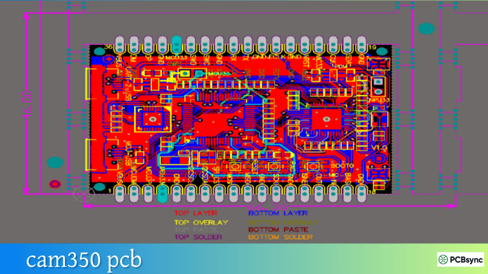
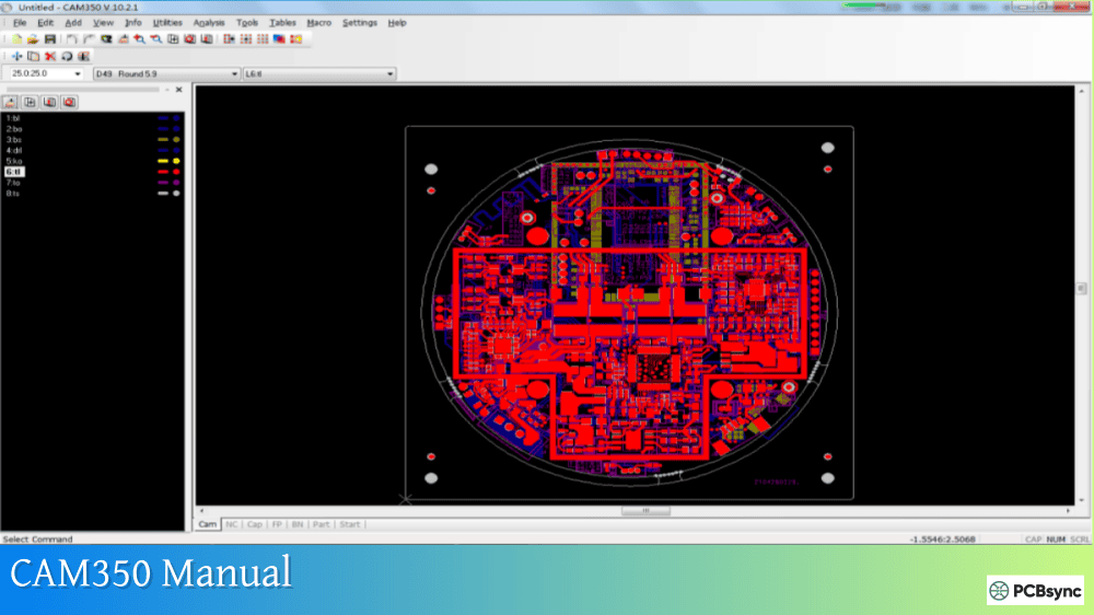
Before diving into the workflow, let’s clarify what we’re working with. Gerber files are the industry standard format for communicating PCB fabrication data. Each file represents a single layer of your PCB—copper layers, soldermask, silkscreen, paste mask, and mechanical outlines. When you send files to a manufacturer, they use CAM software to process these files for production.
CAM350 Gerber processing serves two primary audiences: PCB designers verifying their output before release, and fabrication engineers preparing data for production. The software handles import, verification, editing, panelization, and output generation—essentially everything needed to transition from design to manufacturing.
Gerber Format Types Supported in CAM350
Format
Description
Aperture Handling
RS-274X (Extended Gerber)
Modern standard with embedded apertures
Self-contained, no separate file needed
RS-274D (Standard Gerber)
Legacy format requiring separate aperture file
Requires external aperture list
Fire9000
Proprietary format with embedded apertures
Self-contained
Barco DPF
Specialized format
Format-specific handling
For new designs, RS-274X is the recommended format. It embeds aperture definitions within the file itself, eliminating the compatibility issues that plague RS-274D workflows. If you’re exporting from modern CAD tools like Altium Designer, KiCad, or Cadence Allegro, always select RS-274X.
Step 1: Importing Gerber Files into CAM350
The import process is where many engineers first encounter problems. CAM350 offers multiple import methods, each suited to different situations.
Method A: Auto Import (Recommended for Complete Packages)
Auto Import is the fastest way to load a complete Gerber package when all files are in a single directory:
Launch CAM350 and select File → Import → AutoImport
Navigate to the directory containing your Gerber files
CAM350 scans the folder and identifies file types automatically
Review the file list—by default, do not select drill files yet (import these separately)
Click Finish to complete the import
Important tip: Import drill data separately using File → Import → Drill Data. This gives you better control over drill format settings, particularly the Leading/Trailing zero suppression that causes alignment issues if mismatched.
When you need precise control over what gets loaded:
Select File → Import → Gerber Data
Choose the specific files you want to import
In the import dialog, configure:
Units (Imperial/Metric)
Format (typically 2:4 or 2:5 for inches, 3:3 for metric)
Zero suppression (Leading or Trailing)
Aperture source (Auto-detect for RS-274X)
Import Settings Reference Table
Setting
Common Values
Notes
Units
Inches / Millimeters
Must match source CAD export
Integer Places
2-4
Defines coordinate precision
Decimal Places
3-6
Higher = more precision
Zero Suppression
Leading / Trailing
Must match export settings exactly
Aperture Format
RS-274X / Auto-detect
Use Auto-detect when unsure
Step 2: Importing Drill Files Separately
Drill file handling in Gerber CAM350 workflows requires special attention because misaligned drill data causes catastrophic fabrication errors.
Go to File → Import → Drill Data
Click the browse button and select your drill file (.drl, .txt, .xln, or .exc)
Choose All Files in the filter to see all available files
Select the correct format:
Leading zero suppression (most common)
Trailing zero suppression
Explicit decimal point
Click OK to import
After import, visually verify drill alignment by overlaying the drill layer on your top copper layer. Pad centers should align perfectly with drill hits. If they don’t, you have a format mismatch that needs correction.
Step 3: Layer Alignment and Setup
Once data is loaded, proper layer setup ensures accurate verification and output. This step in the CAM350 Gerber workflow catches issues that would otherwise reach production.
Aligning Layers
If layers appear offset from each other:
Select Edit → Layers → Align
Choose a reference point common to all layers (typically a board corner or tooling hole)
Apply alignment to bring all layers into registration
Setting the Origin
Establish a consistent datum for measurements and panelization:
Go to Edit → Change → Origin → Datum Coordinate
Click on your desired origin point (typically lower-left board corner)
All coordinates will now reference this point
Layer Ordering
Organize layers in a logical stackup order:
Select Edit → Layers → Reorder
Drag layers into proper sequence (Top → Inner → Bottom)
Delete any unused or empty layers
Standard PCB Layer Designations
Extension
Layer Type
Description
.GTL
Top Copper
Top signal layer
.GBL
Bottom Copper
Bottom signal layer
.GTS
Top Soldermask
Top solder resist
.GBS
Bottom Soldermask
Bottom solder resist
.GTO
Top Silkscreen
Top overlay/legend
.GBO
Bottom Silkscreen
Bottom overlay/legend
.GTP
Top Paste
Top stencil layer
.GBP
Bottom Paste
Bottom stencil layer
.GKO/.GML
Board Outline
Mechanical/keepout layer
.DRL
Drill File
NC drill data
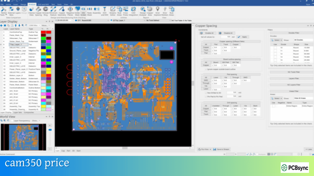
Step 4: Running Design Rule Checks (DRC)
The DRC function in CAM350 Gerber processing identifies spacing violations, minimum feature sizes, and other rule violations before they become production problems.
Basic DRC Procedure
Navigate to Analysis → DRC
Configure check parameters based on your fab house capabilities:
Minimum trace width
Minimum spacing
Minimum annular ring
Minimum drill size
Select layers to check
Run the analysis
Key DRC Parameters to Verify
Check Type
Typical Minimum
What It Catches
Trace Width
4-6 mil
Narrow traces that may open
Trace Spacing
4-6 mil
Shorts between conductors
Annular Ring
4-5 mil
Breakout risk on pads
Drill to Copper
8-10 mil
Shorts to internal layers
Solder Mask Sliver
4 mil
Mask adhesion problems
Review each error in the results list. CAM350 highlights violations on the design, making it easy to locate and assess each issue.
Step 5: DFM Analysis for Manufacturing Verification
Beyond basic DRC, Design for Manufacturing analysis in Gerber CAM350 evaluates your design against real production capabilities.
Running DFM Streams
Select Analysis → Streams RC (or use the Streams toolbar)
Choose or create a stream file containing your checks
Include tests for:
Acid traps (acute copper angles)
Copper slivers (thin copper features)
Soldermask slivers
Thermal relief issues
Solder bridge potential
Execute the stream and review results
DFM analysis catches issues that pass DRC but still cause production problems. Acid traps, for example, might meet spacing rules but trap etchant and cause copper defects.
Step 6: Netlist Comparison and Verification
Netlist compare is the most critical verification step in CAM350 Gerber processing. It confirms that your Gerber data matches the original design intent by checking electrical connectivity.
Netlist Compare Process
Import your reference netlist (IPC-D-356 format is preferred):
File → Import → Netlist
Select the IPC-D-356 file from your CAD export
Extract a netlist from your Gerber data:
Utilities → Netlist Extract
Accept default settings for basic extraction
Run the comparison:
Analysis → Compare Netlists
Select both the imported reference and extracted netlists
Review results for:
Open circuits (broken connections)
Short circuits (unintended connections)
Missing nets
Extra nets
Preparing Data for Accurate Netlist Extraction
For reliable netlist extraction from Gerber CAM350:
Ensure all layers are properly aligned
Verify drill data is correctly loaded and positioned
For blind/buried vias, define layer sets correctly in Home → Panes → Layer Sets
Convert drawn pads to flashes if needed: Tools → Draw to Flash
Step 7: Editing Gerber Data in CAM350
CAM350 allows direct modification of Gerber data—useful for fixing minor issues without returning to the source CAD system.
Common Editing Operations
Adding or Modifying Features:
Select Edit → Add to place new flashes, lines, or polygons
Use RS-274X (Extended Gerber) whenever possible. This format embeds aperture definitions within the file, eliminating the compatibility issues common with RS-274D. All modern PCB CAD tools support RS-274X export. The older RS-274D format requires a separate aperture file, and any mismatch between the Gerber and aperture files causes import failures. When working with CAM350 Gerber data from unknown sources, try Auto-detect apertures first.
How do I fix drill misalignment in CAM350?
Drill misalignment typically results from format mismatches between the drill file and Gerber data. First, check that units match (inches vs. millimeters). Then verify the coordinate format—if your Gerber uses 2:4 format, your drill file should match. Finally, confirm zero suppression settings (Leading vs. Trailing). Re-import the drill file with corrected settings, then overlay on copper to verify alignment. Use Edit → Layers → Align if minor adjustment is needed.
Can CAM350 convert Gerber files back to CAD format?
Yes, CAM350 includes Reverse Engineering capability in higher configurations. This feature converts non-intelligent Gerber data back into a structured format with defined traces, vias, padstacks, and nets. The process involves building parts, extracting netlists, and exporting to CAD formats like PADS ASCII or GenCAD. However, the result requires significant cleanup and should be considered a starting point rather than a finished design. It’s most useful for legacy designs where original CAD data is lost.
Why does netlist extraction show errors when my design is correct?
Netlist extraction problems in Gerber CAM350 usually stem from data preparation issues rather than actual design errors. Common causes include: drawn pads instead of flashes (run Draw to Flash conversion), misaligned layers (check alignment), missing or incorrect drill data (verify drill import settings), and undefined layer sets for blind/buried vias. Address these data issues before re-running extraction. Also ensure you’re using an IPC-D-356 netlist for comparison rather than a reference-designator-based netlist.
What’s the difference between DRC and DFM analysis in CAM350?
DRC (Design Rule Check) verifies basic geometric rules like minimum trace width, spacing, and annular ring. These are pass/fail checks against specific numeric values. DFM (Design for Manufacturing) analysis goes deeper, identifying features that might pass DRC but still cause production problems—acid traps, copper slivers, thermal relief issues, and potential solder bridges. Think of DRC as checking the rules and DFM as checking manufacturability. Both are essential steps in the CAM350 Gerber verification workflow.
Conclusion
Mastering CAM350 Gerber processing takes practice, but the payoff is substantial—fewer fabrication issues, faster turnaround, and more reliable products. The workflow I’ve outlined here covers the essential steps: proper import with format matching, layer alignment and setup, DRC and DFM verification, netlist comparison, editing when necessary, and clean export for production.
The most common problems I see come from format mismatches during import and skipped verification steps. Take the time to verify drill alignment, run DRC checks, and compare netlists before releasing files to manufacturing. These steps catch issues that would otherwise become expensive production problems.
Whether you’re a designer verifying output or a CAM engineer preparing production files, these Gerber CAM350 techniques will improve your results and streamline your workflow.
Inquire: Call 0086-755-23203480, or reach out via the form below/your sales contact to discuss our design, manufacturing, and assembly capabilities.
Quote: Email your PCB files to Sales@pcbsync.com (Preferred for large files) or submit online. We will contact you promptly. Please ensure your email is correct.
Notes: For PCB fabrication, we require PCB design file in Gerber RS-274X format (most preferred), *.PCB/DDB (Protel, inform your program version) format or *.BRD (Eagle) format. For PCB assembly, we require PCB design file in above mentioned format, drilling file and BOM. Click to download BOM template To avoid file missing, please include all files into one folder and compress it into .zip or .rar format.


