Inquire: Call 0086-755-23203480, or reach out via the form below/your sales contact to discuss our design, manufacturing, and assembly capabilities.
Quote: Email your PCB files to Sales@pcbsync.com (Preferred for large files) or submit online. We will contact you promptly. Please ensure your email is correct.
Notes: For PCB fabrication, we require PCB design file in Gerber RS-274X format (most preferred), *.PCB/DDB (Protel, inform your program version) format or *.BRD (Eagle) format. For PCB assembly, we require PCB design file in above mentioned format, drilling file and BOM. Click to download BOM template To avoid file missing, please include all files into one folder and compress it into .zip or .rar format.
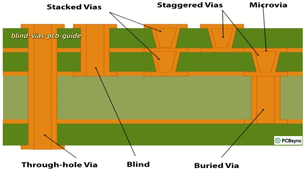
If you have worked on multilayer PCB designs, you know the constant battle for routing space. Through-hole vias punch through every layer of your board, eating up valuable real estate on surfaces where you desperately need room for components and traces. That is where buried vias cohttps://pcbsync.com/multilayer-pcb/me into play.
Buried vias are internal connections that link inner layers of a PCB without ever reaching the outer surfaces. Think of them as underground tunnels in your circuit board—they do their job connecting internal layers while staying completely hidden from the top and bottom of your board. This might sound like a small distinction, but it makes a massive difference when you are trying to squeeze maximum functionality into compact devices.
In this guide, I will walk you through everything you need to know about buried vias PCB design—from understanding what they are and how they differ from other via types, to practical design rules and real-world applications. Whether you are designing your first HDI board or looking to optimize an existing high-density design, this article will give you the engineering perspective you need.
What Are Buried Vias in PCB?
A buried via is a plated through-hole that connects two or more internal layers of a multilayer PCB without extending to either outer surface. Unlike through-hole vias that span the entire board thickness, buried vias remain completely encapsulated within the board structure—hence the name “buried.”
Here is how it works: buried vias are created by drilling and plating the inner layer cores before the complete board stack-up is laminated together. Once the outer layers are added, these connections become invisible from both the top and bottom surfaces.
How Buried Vias Differ from Other Via Types
Understanding the differences between via types is crucial for making the right design decisions. Let me break down the three main categories:
Why go through the extra PCB manufacturing complexity of buried vias? The benefits are substantial for the right applications. Let me explain the key advantages from a practical engineering standpoint.
Increased Routing Density
This is the primary reason most engineers turn to buried vias. Since these connections stay entirely within the inner layers, your outer surfaces remain clear for component placement and additional routing. In dense BGA fanout situations, this can be the difference between a 10-layer board and an 8-layer board—a significant cost and complexity reduction.
Enhanced Signal Integrity
Buried vias help reduce signal path lengths and minimize stub effects that plague through-hole vias in high-speed designs. When a through-hole via only connects to certain layers, the unused portion acts as a stub that reflects signals and degrades performance. Buried vias eliminate this problem by only existing where they are needed.
Additionally, buried vias contribute to lower EMI because they reduce the antenna effect created by long via barrels penetrating unused layers.
Space Optimization
Compared to through-hole vias, buried vias can save up to 50% of surface space in certain configurations. This freed-up real estate allows for more SMT components, better thermal management features, and cleaner power distribution networks.
Improved Aspect Ratio Management
Aspect ratio—the relationship between via depth and diameter—becomes problematic in thick boards. Through-hole vias in a 3mm+ board push the limits of reliable plating. Buried vias solve this by only spanning the layers they connect, keeping aspect ratios manageable even in high layer-count designs.
Benefit
Engineering Impact
Higher Routing Density
Potential 2-layer reduction in board design, saving material and fabrication costs
Better Signal Integrity
Reduced stub effects and EMI, critical for signals above 500MHz
Surface Space Savings
Up to 50% more area available for components and thermal features
Controlled Aspect Ratios
Enables reliable plating in thick, high layer-count boards (20+ layers)
Enhanced Reliability
Protected internal connections less susceptible to environmental stress
Table 2: Summary of Buried Via Benefits
Buried Vias Design Rules and Guidelines
Getting buried vias right requires attention to specific design parameters. Here are the critical rules I follow in my designs, based on IPC standards and real-world manufacturing feedback.
Aspect Ratio Requirements
The aspect ratio—via depth divided by via diameter—is your most critical parameter. For buried vias, IPC standards and most manufacturers require:
Recommended aspect ratio: 1:1 or better (depth ≤ diameter)
Maximum aspect ratio: 1:12 for standard processes
For stacked configurations: Keep aspect ratio at 0.8:1 or better
Higher aspect ratios lead to plating issues—the copper cannot adequately coat the via walls, creating reliability problems.
Minimum Via Dimensions
According to IPC standards, buried vias should have:
Minimum diameter: 0.15mm (6 mils) for mechanical drilling
Understanding how buried vias are manufactured helps you make better design decisions and communicate effectively with your fabricator. The process is more complex than standard PCB fabrication, which is why costs are higher.
Sequential Lamination Process
Sequential lamination is the standard method for creating buried vias. Unlike traditional lamination where all layers are bonded simultaneously, sequential lamination builds the board in stages:
Step 1 – Core Preparation: Individual inner layer cores are fabricated with their circuit patterns
Step 2 – Drilling: Buried via holes are mechanically drilled in the inner cores before lamination
Step 3 – Plating: Drilled holes are copper plated to create conductive connections
Step 4 – Via Fill: Vias are filled with conductive or non-conductive epoxy to prevent air entrapment
Step 5 – First Lamination: Inner cores with buried vias are bonded together using prepreg
Step 6 – Additional Layers: Outer layers are added in subsequent lamination cycles
Step 7 – Final Processing: Through-holes are drilled, plated, and surface finishes applied
Mechanical vs. Laser Drilling
For buried vias, mechanical drilling is the standard approach since the vias are created before lamination. Laser drilling is typically reserved for blind microvias created after lamination. The choice affects minimum via sizes:
Mechanical drilling: Minimum 0.15mm (6 mils) diameter, suitable for most buried via applications
Laser drilling: Down to 0.1mm (4 mils), used for microvias in HDI sequential build-ups
Quality Control and Inspection
Because buried vias are hidden within the board, inspection requires specialized techniques:
X-Ray Inspection: Non-destructive method to verify via alignment and detect voids
Microsectioning: Destructive testing on sample boards to measure plating thickness and via integrity
Electrical Testing: Continuity and isolation tests to verify all connections
Cost Considerations: Buried Vias vs. Standard Vias
Let me be direct: buried vias cost more. But the question is whether they provide enough value to justify that cost in your specific application.
Cost Factors
Several factors drive the increased cost of buried via PCBs:
Manufacturing Complexity: Sequential lamination adds 20-30 processing steps compared to standard fabrication
Equipment Requirements: Specialized drilling and alignment equipment is required
Yield Impact: More process steps mean more opportunities for defects
Inspection Costs: X-ray and microsection testing add to quality control expenses
Typical Cost Premium
Based on industry data and manufacturer feedback:
Buried vias typically increase PCB costs by 20-50% over through-hole only designs
Complex HDI boards with buried vias: $2-10 per square inch vs. $1-5 for standard boards
Some manufacturers quote 200-500% premium for blind/buried via boards vs. standard multilayer
When Buried Vias Save Money
Counterintuitively, buried vias can reduce total costs in specific scenarios:
Layer Count Reduction: If buried vias let you eliminate 2+ layers, the savings may exceed the via premium
Board Size Reduction: Smaller boards mean more boards per panel, reducing per-unit costs
Yield Improvement: Better aspect ratios in thick boards can improve manufacturing yield
The break-even point typically occurs around 20+ layer boards or when significant layer count reduction is achievable.
When to Use Buried Vias: Applications and Use Cases
Buried vias are not for every project. Here are the scenarios where they make the most sense.
Consumer Electronics
Smartphones, tablets, wearables, and laptops rely heavily on buried via technology. The relentless push for thinner, lighter devices with more functionality makes buried vias essential for managing component density in limited board space.
Medical Devices
Implantable devices, diagnostic equipment, and monitoring systems benefit from the compact, reliable designs enabled by buried vias. Medical applications also value the enhanced reliability of protected internal connections.
Aerospace and Defense
Avionics, radar systems, satellite communications, and control systems demand the reliability and space efficiency that buried vias provide. Weight and space constraints in aerospace make every millimeter count.
Automotive Electronics
Advanced driver assistance systems (ADAS), infotainment units, and engine control modules increasingly use HDI technology with buried vias. The automotive environment demands reliable connections that can withstand vibration and temperature cycling.
High-Speed Computing
Servers, GPUs, and AI/ML hardware require excellent signal integrity at high data rates. Buried vias help manage signal path lengths and reduce interference in these demanding applications.
Industry
Applications
Key Driver
Consumer Electronics
Smartphones, tablets, wearables
Miniaturization, high density
Medical
Implants, diagnostics, monitoring
Reliability, compact size
Aerospace
Avionics, satellites, radar
Weight reduction, reliability
Automotive
ADAS, infotainment, ECUs
Harsh environment reliability
Computing
Servers, GPUs, AI hardware
Signal integrity, high speed
Telecom
5G infrastructure, base stations
High-frequency performance
Table 4: Buried Via Applications by Industry
Best Practices for Buried Via PCB Design
After years of working with buried vias, here are the practices that consistently lead to successful designs:
Engage Your Manufacturer Early
Do not finalize your stack-up without consulting your fabricator. Manufacturing capabilities vary significantly—some shops handle 0.1mm vias with 0.2mm spacing, while others require 0.3mm or more. Get their DFM guidelines before you start routing.
Plan Layer Stack-up Before Routing
Define your buried via spans and layer assignments before placing a single component. Changing via spans mid-design often requires significant rework. Use your CAD tool’s stack-up manager to document via spans clearly.
Avoid Stacking on Mechanical Buried Vias
Stacking a microvia directly on top of a mechanically drilled buried via is a known reliability issue. The structure is prone to cracking. If you need stacked connections, offset your laser-drilled vias from the buried via and stack from that point.
Use Via Fill for All Buried Vias
Always specify via fill (conductive or non-conductive epoxy) for buried vias. Unfilled vias can trap air during lamination, leading to voids and reliability problems. Most manufacturers will do this automatically, but specify it explicitly.
Document Everything
Create separate drill files for each buried via span. Include a detailed fabrication drawing showing the layer stack-up, via spans, and any special requirements. Clear documentation prevents manufacturing errors and reduces review cycles.
Useful Resources for Buried Via Design
Here are the standards and tools I recommend for anyone working with buried vias:
IPC Standards
IPC-2221B: Generic Standard on Printed Board Design – covers via design fundamentals
IPC-2226: Sectional Design Standard for HDI Printed Boards – essential for HDI designs
IPC-4761: Design Guide for Protection of Printed Board Via Structures – via fill types
IPC-6012: Qualification and Performance Specification for Rigid PCBs – acceptance criteria
Design Tools and Calculators
Via aspect ratio calculators (available from most CAD vendors)
Stack-up impedance calculators (Saturn PCB Toolkit is free)
HDI cost estimators from major fabricators
Industry Resources
For the latest updates on HDI design practices and buried via technology, the IPC website provides standards and technical resources. Major PCB design software vendors like Altium, Cadence, and Mentor also publish extensive HDI design guides.
Frequently Asked Questions About Buried Vias PCB
1. What is the difference between buried vias and blind vias?
Buried vias connect only inner layers and are invisible from both outer surfaces. Blind vias connect an outer layer to one or more inner layers but do not pass through the entire board—they are visible from one side only. Both require sequential lamination, but buried vias are created earlier in the manufacturing process before outer layers are added.
2. How much do buried vias add to PCB cost?
Buried vias typically increase manufacturing costs by 20-50% compared to through-hole-only designs. Some manufacturers quote premiums of 200-500% for complex blind/buried configurations. However, if buried vias allow you to reduce layer count or board size significantly, the total cost may actually decrease. Always get quotes for both approaches.
3. What is the minimum size for buried vias?
Per IPC standards, buried vias should have a minimum diameter of 0.15mm (6 mils) when mechanically drilled. The minimum annular ring should be 0.1mm on each side. For HDI designs using laser drilling, microvias can go down to 0.1mm (4 mils), but these are typically blind vias rather than true buried vias.
4. Can buried vias be stacked?
Stacking microvias directly on mechanically drilled buried vias is not recommended—this structure has known reliability issues and can fail under thermal stress. If you need stacked connections, the best practice is to offset your laser-drilled microvias from the buried via location and then stack from that offset point.
5. When should I use buried vias instead of through-hole vias?
Consider buried vias when you face routing density challenges that cannot be solved with through-hole vias, when you need to reduce layer count in a high-complexity design, when signal integrity requirements demand shorter via lengths, or when your board thickness creates aspect ratio problems for through-holes. For simpler designs or cost-sensitive projects, through-hole vias remain the better choice.
Conclusion
Buried vias are a powerful tool in the PCB designer’s toolkit, enabling higher density, better signal integrity, and more compact designs. They are essential for modern HDI applications in consumer electronics, medical devices, aerospace, automotive, and high-speed computing.
However, buried vias are not always the right choice. The added manufacturing complexity and cost mean you should carefully evaluate whether the benefits justify the investment for your specific application. In many cases, creative routing with standard through-hole vias can achieve acceptable results at lower cost.
The key to success with buried vias is planning. Engage your manufacturer early, define your via spans before routing, and document your requirements clearly. With proper planning and adherence to design rules, buried vias will help you create high-performance PCBs that meet the demands of today’s most challenging applications.
If you are working on an HDI design or facing routing challenges in a multilayer board, I encourage you to explore whether buried vias might be the solution. The upfront investment in understanding this technology pays dividends in design flexibility and product performance.
Inquire: Call 0086-755-23203480, or reach out via the form below/your sales contact to discuss our design, manufacturing, and assembly capabilities.
Quote: Email your PCB files to Sales@pcbsync.com (Preferred for large files) or submit online. We will contact you promptly. Please ensure your email is correct.
Notes: For PCB fabrication, we require PCB design file in Gerber RS-274X format (most preferred), *.PCB/DDB (Protel, inform your program version) format or *.BRD (Eagle) format. For PCB assembly, we require PCB design file in above mentioned format, drilling file and BOM. Click to download BOM template To avoid file missing, please include all files into one folder and compress it into .zip or .rar format.


