Inquire: Call 0086-755-23203480, or reach out via the form below/your sales contact to discuss our design, manufacturing, and assembly capabilities.
Quote: Email your PCB files to Sales@pcbsync.com (Preferred for large files) or submit online. We will contact you promptly. Please ensure your email is correct.
Notes: For PCB fabrication, we require PCB design file in Gerber RS-274X format (most preferred), *.PCB/DDB (Protel, inform your program version) format or *.BRD (Eagle) format. For PCB assembly, we require PCB design file in above mentioned format, drilling file and BOM. Click to download BOM template To avoid file missing, please include all files into one folder and compress it into .zip or .rar format.
Boundary Scan Testing (JTAG) in PCB Design: A Practical DFT Guide
If you’ve ever stared at a 400-ball BGA wondering how you’re supposed to verify those solder joints without X-ray, you understand why boundary scan testing exists. After years of bringing up boards with increasingly fine-pitch components and shrinking test point real estate, I’ve come to appreciate JTAG not just as a programming interface, but as an essential test methodology that should be designed in from day one.
This guide covers boundary scan testing from a design-for-testability perspective, including the practical implementation details that determine whether your JTAG chain actually works on the bench.
Boundary scan testing is a method for testing interconnects between integrated circuits on a PCB without requiring physical probe access to every signal. The technique embeds shift-register cells at each I/O pin of a compliant device, allowing test signals to be driven and sensed through a standardized four-wire serial interface.
The Joint Test Action Group (JTAG) developed the original specification in the 1980s to address a fundamental problem: surface-mount technology and ball grid array packages made traditional bed-of-nails testing impractical. The IEEE standardized the approach as IEEE 1149.1 in 1990, and it’s been evolving since.
Here’s what makes boundary scan testing different from other approaches: instead of probing traces externally, you access circuit nodes from inside the devices themselves. Each boundary scan cell can capture the state of its pin or force a value onto it. String all these cells together across multiple devices, and you have a virtual probe that can reach connections that would otherwise be completely inaccessible.
How Boundary Scan Works
The boundary scan architecture consists of several key elements built into each compliant IC:
Boundary Scan Register (BSR): A shift register chain connecting all I/O pins. In normal operation, these cells are transparent. During testing, they intercept signals between the device core and its pins.
Test Access Port (TAP): The standard four-wire (optionally five-wire) interface that controls the boundary scan logic.
TAP Controller: A state machine that responds to the TMS signal and coordinates test operations.
Instruction Register: Holds the current test instruction, determining which operation the device performs.
During a boundary scan testing sequence, the tester shifts data into the boundary scan register through TDI, applies it to the device pins, captures the results, and shifts them out through TDO. By comparing captured values against expected results, the system identifies shorts, opens, and other interconnect faults.
Understanding the JTAG Test Access Port
The TAP interface is your entry point for all boundary scan testing operations. Understanding these signals is essential for proper PCB design.
Signal
Name
Direction
Function
TCK
Test Clock
Input
Clock for all test operations
TMS
Test Mode Select
Input
Controls TAP state machine
TDI
Test Data In
Input
Serial data input
TDO
Test Data Out
Output
Serial data output
TRST
Test Reset
Input (Optional)
Asynchronous reset of TAP controller
TCK and TMS are broadcast to all devices in parallel. TDI and TDO form a daisy chain, with TDO from one device connecting to TDI of the next. This creates a single scan path through all boundary scan compliant devices on the board.
Key IEEE 1149.x Standards
The boundary scan ecosystem has grown beyond the original 1149.1 specification:
Standard
Purpose
Application
IEEE 1149.1
Original boundary scan
Digital interconnect testing
IEEE 1149.4
Mixed-signal test bus
Analog and mixed-signal testing
IEEE 1149.6
AC-coupled signals
High-speed differential interfaces
IEEE 1149.7
Reduced pin count
Two-wire JTAG interface
IEEE 1532
In-system configuration
CPLD/FPGA programming
For most designs, IEEE 1149.1 compliance is the baseline. If your board includes high-speed differential interfaces with AC coupling capacitors, 1149.6 capable devices allow those nets to be tested as well.
What Faults Can Boundary Scan Testing Detect?
Boundary scan testing excels at finding assembly defects that affect digital interconnects:
Solder shorts occur when adjacent pins or traces are bridged by excess solder. The test detects these by driving different values on adjacent nets and checking whether they maintain their distinct states.
Open connections result from insufficient solder, cracked joints, or broken traces. Opens prevent driven values from reaching destination pins, causing captured values to differ from expectations.
Stuck-at faults happen when a net is permanently tied high or low, often due to shorts to power or ground planes.
Missing components show up as open connections on all device pins.
Wrong or reversed components may cause unexpected behavior patterns during interconnect testing.
The technique identifies these faults to pin-level resolution, pointing directly at the specific net, device, and pin involved. This diagnostic precision is what makes boundary scan testing valuable in production—a technician can go straight to the fault location rather than spending hours with a multimeter.
Fault Coverage Considerations
Boundary scan can’t test everything. Its coverage depends on how much of your design connects JTAG-compliant devices to each other:
Full coverage nets: Both ends connect to boundary scan enabled pins.
Partial coverage nets: One end connects to a boundary scan pin, the other to a non-compliant device. You can drive or sense from the compliant end but not both.
No coverage nets: Neither end has boundary scan capability. These require traditional test methods.
Typical designs achieve 50-80% boundary scan coverage without specific optimization. With careful component selection and DFT practices, coverage above 90% is achievable for digital sections of mixed-signal boards.
Design for Testability: JTAG Implementation Guidelines
Getting boundary scan testing right starts in the design phase, not after you’ve already laid out the board. Here are the DFT rules that actually matter.
Component Selection
Select IEEE 1149.1 compliant devices whenever possible. Every compliant device you add increases your potential test coverage. Most modern processors, FPGAs, CPLDs, and complex digital ICs support boundary scan. Even if you don’t plan to use JTAG for production testing, having the capability available for debug is valuable.
Verify BSDL file availability. The Boundary Scan Description Language file describes how the device’s boundary scan logic works. Without accurate BSDL files, your test tools can’t generate valid test patterns. Request these from device manufacturers early in your design process.
Check for 1149.6 support on high-speed interfaces. If your design includes AC-coupled differential signals (common with Ethernet, LVDS, or SerDes interfaces), devices with 1149.6 capability allow those connections to be tested.
Scan Chain Architecture
In the simplest configuration, all JTAG devices on a board connect in a single daisy chain. TDO from device 1 connects to TDI of device 2, and so on. This works well for many designs, but there are reasons to consider alternatives:
Single chain advantages: Simple to implement, requires only one test connector, easy to manage in test software.
Multiple chain considerations: Separate chains for devices with different voltage levels, partition chains for optional populated components, isolate problematic devices that might disrupt testing.
If your board includes optional daughter cards or modules, route the scan chain through these connectors with bypass provisions for when they’re absent. Use jumper networks or multiplexer logic to enable bypassing unpopulated chain segments.
TAP Signal Routing
Poor signal integrity on TAP lines is a common cause of mysterious JTAG failures. These guidelines help avoid problems:
Keep TAP traces short and direct. The serial interface typically runs at 10-30 MHz, but poor layout can still cause errors that are extremely difficult to diagnose.
Terminate TCK appropriately. Use series resistors (33-100 ohms typical) near the test connector to reduce reflections. For long traces or heavily loaded TCK lines, consider proper termination to match trace impedance.
Add pull-up resistors on TMS and TDI. These ensure defined states when the test connector is not attached. 4.7k to 10k ohms to the TAP supply voltage is typical.
Pull TDO low or leave floating depending on your test equipment requirements.
Handle TRST carefully. If present, this signal should have a pull-up to keep the TAP controller out of reset during normal operation. Never connect TRST directly to ground, as this permanently disables the entire chain.
Route TAP signals away from high-speed or noisy traces. Interleaving with ground signals can help reduce crosstalk.
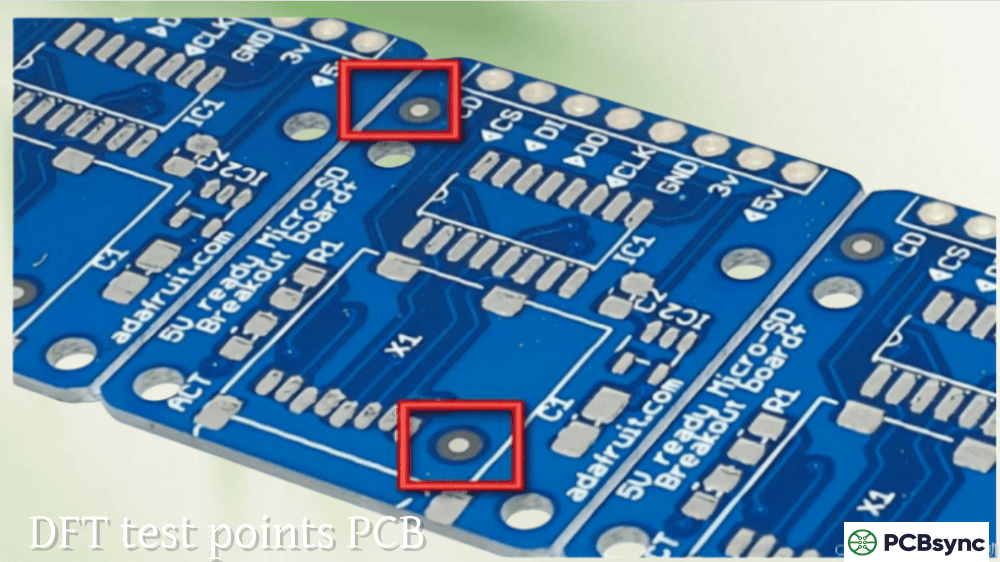
Test Connector Placement
Put the JTAG header at the board edge where test equipment can easily access it. Standard 2.54mm headers work for bench testing; consider smaller pitch for production fixtures.
Use a keyed connector or asymmetric pinout to prevent incorrect cable installation. A cable plugged in backward can short power rails and damage components.
Standardize your connector pinout across designs. This allows reuse of cables and simplifies technician training.
Common pinouts include the ARM 10-pin and 20-pin JTAG headers, which have defined locations for TAP signals, power, and ground. Even if you’re not using ARM processors, adopting a standard pinout makes sense.
Boundary Scan Test Types
Boundary scan testing encompasses several distinct test modes:
Infrastructure Test
Also called chain integrity test, this verifies that the JTAG chain itself is functional. The test reads device ID codes and confirms all expected devices are present and responding. This catches chain breaks, missing devices, and wrong components before attempting more detailed testing.
Interconnect Test (EXTEST)
The primary application of boundary scan testing for manufacturing. EXTEST mode isolates device cores and uses boundary scan cells to drive and capture values on every testable net. Sophisticated algorithms detect and diagnose shorts, opens, and stuck faults between devices.
Internal Test (INTEST)
INTEST applies test vectors to the device core from the boundary scan register, testing internal logic rather than external connections. This is less commonly used in production testing but can be valuable for bringing up new silicon.
In-System Programming
JTAG provides a standard interface for programming FPGAs, CPLDs, and flash memories after board assembly. IEEE 1532 extends this capability with additional features for configuration management.
Functional Test (RUNBIST)
Some devices include built-in self-test logic that can be triggered through JTAG. This extends test coverage to internal structures that boundary scan alone can’t reach.
Integrating Boundary Scan with Other Test Methods
Boundary scan testing rarely stands alone in a complete test strategy. It complements other methods:
Automated Optical Inspection (AOI) catches visible defects like missing components, tombstoning, and solder bridges before electrical testing. It doesn’t verify electrical function.
In-Circuit Test (ICT) uses bed-of-nails fixtures to probe individual nodes and test components. ICT provides excellent coverage for non-JTAG portions of a design but requires physical access points.
Functional Test verifies that the complete system operates correctly. It catches defects that structural tests miss but provides poor fault isolation.
A practical test flow might sequence these methods:
AOI after reflow to catch gross assembly defects
Boundary scan to verify digital interconnects and program devices
ICT for analog sections and non-JTAG components
Functional test for final validation
Some test platforms, like Keysight’s 3070 series, integrate boundary scan capability directly into the ICT system, allowing both methods to run from a single fixture.
Boundary Scan Testing Tools and Resources
Commercial Test Platforms
Vendor
Product
Type
XJTAG
XJDeveloper, XJRunner
Development and production
Corelis
ScanExpress
Development and production
JTAG Technologies
JTAGLive
Development and production
Goepel Electronic
SYSTEM CASCON
Enterprise solutions
Keysight
x1149
ICT integrated
Flynn Systems
onTAP
Automated test generation
Useful Resources and Downloads
Resource
Description
Link
IEEE 1149.1 Standard
Official specification
ieee.org
BSDL Syntax Checker
Free online BSDL validation
goepel.com/bsdl-syntax-checker
XJTAG DFT Assistant
Free testability analysis plugin for OrCAD
xjtag.com
JTAG Technologies DFT Guidelines
Comprehensive design guide
jtag.com
Corelis Boundary Scan Tutorial
Technical introduction
corelis.com/education/tutorials
SVF Specification
Serial Vector Format for test interchange
Asset InterTech
BSDL File Sources
BSDL files are typically available from device manufacturers’ websites. Check the device’s product page under documentation or downloads. Some aggregated sources exist, but always verify BSDL files match your specific device revision.
Having debugged plenty of non-functional scan chains, here are the issues I see repeatedly:
Floating TRST pins: If your device has TRST and you leave it unconnected, noise can randomly reset the TAP controller. Add a pull-up.
Missing pull resistors on TMS/TDI: Without these, the chain may work when test equipment is connected but fail when you try to operate the board normally.
Dual-function TAP pins configured wrong: Some devices allow TAP pins to serve other functions. Configuration typically happens at power-up based on strap pin states. If you configure a device for non-JTAG operation on those pins, it won’t participate in the chain.
Voltage level mismatches: Mixing 3.3V and 1.8V JTAG devices in a chain without level translation causes communication failures or device damage.
No bypass provisions for optional components: If a device might not be populated, you need a way to bypass its position in the chain or the entire chain breaks.
Insufficient TCK drive capability: The TCK line fans out to all devices. Long traces and multiple loads may require buffering.
Frequently Asked Questions About Boundary Scan Testing
What’s the difference between JTAG and boundary scan?
Technically, JTAG (Joint Test Action Group) was the industry consortium that developed the boundary scan standard. IEEE 1149.1 is the actual specification. In practice, the terms are used interchangeably—when someone says “JTAG testing,” they usually mean boundary scan testing. The confusion is compounded because JTAG interfaces are also used for non-boundary-scan purposes like processor debugging and FPGA programming, which use the same physical interface but different protocols.
Can boundary scan testing detect all PCB faults?
No. Boundary scan testing is effective for digital interconnects between compliant devices, but it has blind spots. Analog circuits, connections to non-JTAG components, power supply integrity, and many component-level faults require other test methods. Most production environments combine boundary scan with ICT, AOI, and functional testing for complete coverage.
How much does boundary scan testing add to production time?
Boundary scan tests typically execute in seconds to tens of seconds, depending on board complexity and scan chain length. Programming operations take longer, especially for large FPGAs or flash devices. Compared to comprehensive ICT or functional testing, boundary scan is often faster and can run without expensive custom fixtures, potentially reducing overall test time and cost.
Do I need boundary scan if I’m already doing ICT?
They complement each other. Boundary scan tests interconnects that ICT can’t reach—particularly BGA connections and fine-pitch devices where probe access is impossible. ICT tests analog components and non-JTAG device connections that boundary scan can’t see. Many production lines use both methods together for maximum coverage.
What happens if one device in the scan chain fails?
A broken scan chain typically prevents testing of all devices after the failure point. This is why chain integrity testing runs first—it quickly identifies if and where the chain is broken. Proper DFT design includes bypass provisions for devices that might fail or not be populated, allowing the rest of the chain to remain testable.
Making Boundary Scan Work in Your Design
Implementing effective boundary scan testing requires commitment during the design phase, not as an afterthought. The decisions you make about component selection, chain architecture, and connector placement determine whether you’ll have a useful test capability or a debugging nightmare.
Start by evaluating your design’s testability early. How many of your complex ICs support boundary scan? What percentage of critical nets connect JTAG-compliant devices? Where are your coverage gaps, and how will you address them?
Work with your test engineering team or contract manufacturer before finalizing the design. They can identify potential issues and suggest improvements that are easy to implement during layout but expensive to fix afterward.
The investment in proper DFT pays dividends throughout the product lifecycle: faster bring-up, more efficient production testing, and better field serviceability. For any design with BGAs or fine-pitch components, boundary scan testing capability isn’t optional—it’s the only practical way to verify those connections.
Inquire: Call 0086-755-23203480, or reach out via the form below/your sales contact to discuss our design, manufacturing, and assembly capabilities.
Quote: Email your PCB files to Sales@pcbsync.com (Preferred for large files) or submit online. We will contact you promptly. Please ensure your email is correct.
Notes: For PCB fabrication, we require PCB design file in Gerber RS-274X format (most preferred), *.PCB/DDB (Protel, inform your program version) format or *.BRD (Eagle) format. For PCB assembly, we require PCB design file in above mentioned format, drilling file and BOM. Click to download BOM template To avoid file missing, please include all files into one folder and compress it into .zip or .rar format.


