Inquire: Call 0086-755-23203480, or reach out via the form below/your sales contact to discuss our design, manufacturing, and assembly capabilities.
Quote: Email your PCB files to Sales@pcbsync.com (Preferred for large files) or submit online. We will contact you promptly. Please ensure your email is correct.
Notes: For PCB fabrication, we require PCB design file in Gerber RS-274X format (most preferred), *.PCB/DDB (Protel, inform your program version) format or *.BRD (Eagle) format. For PCB assembly, we require PCB design file in above mentioned format, drilling file and BOM. Click to download BOM template To avoid file missing, please include all files into one folder and compress it into .zip or .rar format.
A practical engineering guide covering blind via PCB design rules, manufacturing processes, aspect ratios, cost considerations, and real-world applications in HDI boards.
Introduction
If you’ve worked on any high-density PCB design recently, you’ve probably hit a wall — literally. You’re trying to route signals under a fine-pitch BGA, and there’s simply no room for through-hole vias. The traces need to escape to inner layers, but standard vias consume space on every layer they pass through, even layers where you don’t need them.
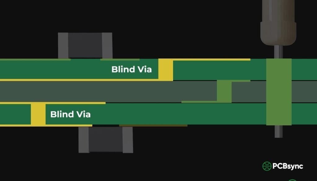
This is exactly where blind vias come in. A blind via connects an outer layer of a PCB to one or more inner layers without passing through the entire board. Unlike through-hole vias that punch from top to bottom, blind vias are visible from only one side — hence the name “blind.”
In this guide, I’ll walk through everything you need to know about blind vias in PCB design: when to use them, how to design them correctly, the manufacturing processes involved, and honest cost considerations. Whether you’re working on smartphones, medical devices, or aerospace electronics, this guide will help you make informed decisions about implementing blind vias in your next project.
A blind via is a plated-through hole that connects an external layer (top or bottom) to one or more internal layers without extending through the entire PCB stack-up. According to IPC-A-600G, blind vias extend from the surface and connect the surface layer with one or more internal layers.
Think of it this way: if you hold a PCB up to a light source, through-hole vias let light pass straight through. Blind vias don’t — they terminate inside the board, making them invisible from the opposite side.
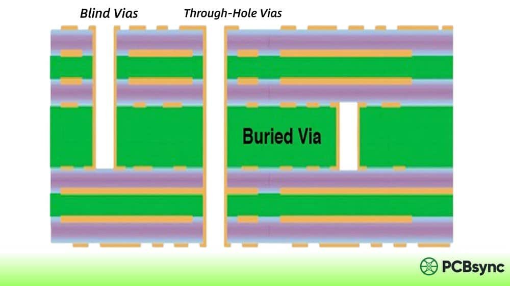
Blind Vias vs. Buried Vias vs. Through-Hole Vias
Understanding the distinction between via types is fundamental to PCB design. Here’s a clear comparison:
In practical terms, if you need to connect a surface-mount BGA pad to an internal signal layer while keeping the bottom layer free for other routing, a blind via from Layer 1 to Layer 2 (on a 6-layer board) accomplishes exactly that.
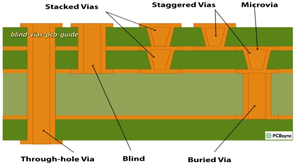
Types of Blind Vias
Not all blind vias are created equal. The manufacturing method you choose significantly impacts hole diameter, reliability, and cost. Here are the main types:
Mechanical Blind Vias
Mechanical blind vias are drilled using standard CNC drilling machines with controlled depth. The drill bit is programmed to stop at a specific layer. This is the most straightforward and cost-effective method when via diameter permits — typically 0.15mm (6 mil) minimum.
Best for: Standard multilayer boards where via diameters of 0.15mm or larger are acceptable and aspect ratio requirements are met.
Laser-Drilled Blind Vias (Microvias)
Laser drilling enables much smaller hole diameters — down to 0.075mm (3 mil) or even smaller. According to IPC-T-50M, a microvia is defined as a blind structure with a maximum aspect ratio of 1:1 and a total depth not exceeding 0.25mm (0.010 inches).
Best for: HDI PCBs, fine-pitch BGAs (0.5mm pitch and below), and designs requiring maximum routing density.
Stacked Blind Vias
When you need to span more than two layers but aspect ratios limit single-via depth, stacked vias offer a solution. Multiple blind vias are aligned vertically, each connecting adjacent layer pairs. The lower vias must be filled with conductive material before the next via is drilled on top.
Best for: High layer count HDI designs where signals must transition across multiple layers in a tight footprint.
Staggered Blind Vias
Staggered vias serve a similar purpose to stacked vias but are offset horizontally rather than aligned. This approach is generally more reliable and less expensive than stacking because it doesn’t require via filling between lamination cycles.
Best for: Designs where stacked vias aren’t mandatory, offering a cost-effective alternative for multi-layer transitions.
Type
Min. Diameter
Aspect Ratio
Typical Application
Mechanical
0.15mm (6 mil)
1:1 minimum
Standard multilayer
Laser (Microvia)
0.075mm (3 mil)
0.75:1 to 1:1
HDI, fine-pitch BGA
Stacked
0.075-0.1mm
Per layer: 1:1
High layer count HDI
Staggered
0.075-0.1mm
Per layer: 1:1
Cost-effective multi-layer
Design Guidelines for Blind Vias PCB
Getting blind via design right requires attention to several critical parameters. Here’s what you need to consider:
Aspect Ratio Requirements
The aspect ratio — the ratio of hole depth to diameter — is the single most critical parameter for blind via reliability. For mechanically drilled blind vias, maintain an aspect ratio of 1:1 or larger (meaning the diameter should equal or exceed the depth).
Why does this matter? During electroplating, the plating solution must flow into the hole and deposit copper uniformly on the barrel walls. Holes that are too deep relative to their diameter create plating challenges — the solution can’t reach the bottom effectively, resulting in thin or inconsistent copper coverage that compromises reliability.
For laser-drilled microvias, the IPC recommends an ideal aspect ratio of 0.75:1, with 1:1 being the maximum. NCAB Group’s design guidelines suggest a typical ratio between 0.6:1 and 1:1, with 0.8:1 being optimal.
Layer Stack-Up Planning
Blind vias must be planned into your layer stack-up from the beginning. Key considerations:
Blind vias should span an even number of copper layers. For example, L1-L2 or L1-L4 on an 8-layer board.
Blind vias must start at an outer layer. By definition, they connect surface layers to inner layers.
Avoid overlapping blind and buried via spans. For example, avoid L1-L3 blind vias simultaneously with L2-L4 buried vias — this dramatically increases PCB manufacturing complexity and cost.
Consider dielectric thickness. The hole depth equals the dielectric thickness plus copper layer thickness. Thicker dielectrics require larger hole diameters to maintain acceptable aspect ratios.
Annular Ring and Pad Sizing
Per IPC standards, the blind via pad should have a diameter at least 300μm (12 mil) larger than the via diameter after copper plating. For laser-drilled vias, this can be reduced to 250μm (10 mil).
Use this formula for pad sizing according to IPC-6012 and IPC-2221:
For IPC Class 3 designs, maintain minimum annular rings of 2 mil on external layers and 1 mil on internal layers. Larger annular rings on inner layers improve connection stability and reliability.
Via-in-Pad Design
Blind vias can be placed directly within component pads — a technique called via-in-pad or VIPPO (Via-in-Pad Plated Over). This is particularly useful for BGA fan-out where escape routing space is limited.
However, via-in-pad requires the vias to be filled and plated over to create a flat, solderable surface. Without proper filling, solder can wick into the via during assembly, creating voids or insufficient solder joints.
Understanding the manufacturing process helps explain why blind vias cost more and how to design for manufacturability.
Sequential Lamination Process
The most common method for creating blind vias involves sequential lamination:
Inner Layer Processing: Inner layers are imaged, etched, and inspected as individual cores.
Sub-Assembly Lamination: Selected layers are laminated together to form a sub-stack.
Blind Via Drilling: Holes are drilled from the outer surface to the target layer using controlled-depth mechanical drilling or laser ablation.
Plating: The drilled holes are cleaned and electroplated with copper to create the conductive path.
Via Filling (if required): For stacked vias or via-in-pad applications, holes are filled with conductive or non-conductive material.
Final Lamination: Remaining layers are laminated to complete the stack-up.
Through-Hole Processing: Standard through-hole vias are drilled and plated.
Drilling Methods Compared
Method
Advantages
Limitations
Cost Impact
Controlled Depth Mechanical
Lower cost, proven technology
Min. 0.15mm diameter, depth tolerance
$0.01-0.05/via
CO2 Laser
Fast, good for larger microvias
Can’t drill through copper directly
$0.05-0.10/via
UV Laser
Smallest holes, high precision
Slowest, highest equipment cost
$0.10-0.15/via
Critical Manufacturing Considerations
Drill Depth Control: Depth tolerance is critical. If the hole is too shallow, it won’t reach the target layer, resulting in an open connection. If too deep, it may penetrate into unintended layers, causing shorts or signal degradation.
Plating Uniformity: The IPC requires minimum copper plating thickness of 20μm average (18μm minimum) for Class 1 and 2, and 25μm average (20μm minimum) for Class 3. Achieving uniform plating at the bottom of blind vias is challenging.
Via Filling: Unfilled blind vias can trap air bubbles during subsequent lamination, leading to voids, delamination, or solder joint failures. Consult with your fabricator about filling requirements.
Signal Integrity Benefits of Blind Vias
For high-speed designs, blind vias offer measurable signal integrity advantages over through-hole vias.
Reduced Via Stub Length
The most significant benefit is eliminating via stubs. When a signal transitions from Layer 1 to Layer 2 using a through-hole via on an 8-layer board, the unused portion of the via barrel from Layer 2 to Layer 8 acts as an antenna stub. This stub creates reflections and resonances that degrade signal quality, particularly at high frequencies.
Research published in IEEE indicates that for signals above 5 Gbps, via stub effects become significant. A blind via from L1-L2 eliminates this stub entirely, maintaining cleaner signal transitions.
Lower Parasitic Capacitance and Inductance
Shorter vias mean lower parasitic capacitance and inductance. The parasitic capacitance of a via is proportional to the barrel length and the proximity to surrounding ground planes. By limiting the via to only the layers needed, you reduce these parasitic effects.
In high-speed designs, this translates to faster rise times, reduced signal attenuation, and improved impedance matching. Some designers report signal propagation delay improvements of 20-30% compared to through-hole vias in certain configurations.
Better EMI Performance
With signals confined to specific layers, blind vias help minimize electromagnetic interference and crosstalk between adjacent traces. This is particularly valuable for high-frequency applications like 5G communications, where frequencies can exceed 28 GHz.
Cost Considerations
Let’s be direct: blind vias add cost. But understanding why and when that cost is justified helps you make smart design decisions.
Why Blind Vias Cost More
Additional Manufacturing Steps: Sequential lamination requires multiple pressing cycles, each adding time and potential yield loss.
Precision Requirements: Controlled-depth drilling and layer-to-layer registration demand tighter tolerances.
Specialized Equipment: Laser drilling for microvias requires expensive equipment with limited throughput.
On average, expect a 10-30% cost increase compared to standard through-hole PCBs, depending on design complexity and via structure requirements.
Production Region
Typical Cost Range
Notes
China
$5-50 per board
Best for volume production
North America
$20-200 per board
Higher for aerospace/military
Europe
$30-250 per board
Strict environmental compliance
Southeast Asia
$10-80 per board
Growing capability
When Blind Vias Can Reduce Overall Cost
Here’s the counterintuitive part: sometimes blind vias actually reduce total PCB cost by enabling:
Layer Count Reduction: By improving routing density, you might reduce an 8-layer through-hole design to a 6-layer HDI design with blind vias. The layer savings can offset the HDI premium.
Board Size Reduction: Smaller blind vias mean more routing channels, potentially allowing a smaller board footprint — directly reducing material costs.
Aspect Ratio Compliance: For thick boards, through-hole vias may exceed aspect ratio limits, requiring larger drill sizes. Blind vias spanning fewer layers maintain favorable aspect ratios with smaller holes.
Applications of Blind Vias in PCB
Blind vias are most commonly found in HDI (High-Density Interconnect) PCBs. Here are the primary application areas:
Consumer Electronics
Smartphones, tablets, and wearables rely heavily on blind vias to achieve the miniaturization consumers expect. The latest smartphone motherboards typically use multiple HDI layers with stacked microvias to route signals from application processors with 0.35-0.5mm pitch BGAs.
Medical Devices
Implantable devices, diagnostic equipment, and surgical instruments demand compact, reliable PCBs. Blind vias enable complex functionality in the small form factors required for patient comfort and safety.
Telecommunications
5G infrastructure equipment, network routers, and high-speed transceivers benefit from the signal integrity advantages of blind vias. Base station PCBs often combine traditional through-hole vias with blind and buried vias to optimize both cost and performance.
Aerospace and Military
Mission-critical applications in avionics and defense systems use blind vias where space and weight constraints are severe. These applications typically follow IPC Class 3 standards with additional reliability requirements per IPC-6012ES.
Automotive Electronics
Advanced driver-assistance systems (ADAS), infotainment units, and EV power electronics increasingly use HDI technology. Blind vias help manage the high component density while meeting automotive reliability requirements under thermal cycling and vibration.
Common Design Mistakes to Avoid
After reviewing hundreds of blind via designs, here are the mistakes I see most often:
Ignoring Aspect Ratio Limits: Designing 0.1mm vias through 0.3mm dielectric creates a 3:1 aspect ratio — far beyond the 1:1 recommended maximum. This leads to plating voids and reliability failures.
Overlapping Blind and Buried Via Spans: Creating blind vias from L1-L3 while also using buried vias from L2-L4 requires complex sequential build-ups that significantly increase cost and reduce yield.
Placing Vias Between SMD Pads: Blind vias placed directly between surface-mount pads can trap flux during assembly, leading to corrosion and reliability issues. The trapped flux is difficult to inspect and clean.
Insufficient Annular Rings: Undersized pads combined with drill wander can result in breakout, creating open connections or weakened joints.
Not Communicating with Your Fabricator: Every fabricator has different capabilities and preferences. Design rules that work at one shop may be outside tolerance at another. Always submit your stack-up for review before finalizing design.
Frequently Asked Questions
What is the minimum hole size for blind vias?
For mechanically drilled blind vias, the practical minimum is 0.15mm (6 mil). Laser-drilled microvias can achieve 0.075-0.1mm (3-4 mil) diameters. IPC standards suggest that blind and buried vias should have diameters of 150μm (6 mil) or less to be classified as microvias.
Can blind vias be used on 4-layer PCBs?
Yes, but it’s less common. On a 4-layer board, blind vias would connect L1-L2 or L3-L4. The cost premium may not be justified unless you have specific routing constraints or fine-pitch components that require them. Evaluate whether through-hole vias can meet your needs first.
How many layers can a blind via span?
Typically, blind vias span 1-2 layers from the surface due to aspect ratio constraints. For example, L1-L2 or L1-L3 on a high-layer-count board. If you need to span more layers, consider stacked or staggered vias, or evaluate whether a buried via combined with through-holes might be more cost-effective.
Do blind vias need to be filled?
It depends on your application. Blind vias under BGA pads (via-in-pad) must be filled and plated over to prevent solder wicking. For vias not under pads, filling is often recommended to prevent air entrapment during subsequent lamination, but may not be required. Consult your fabricator’s guidelines.
What’s the typical lead time for blind via PCBs?
Sequential lamination adds 2-5 days to standard fabrication cycles. Quick-turn prototypes typically take 5-10 business days for simple blind via structures, while complex HDI designs with multiple lamination cycles may require 15-20 days. Always confirm with your fabricator based on specific design complexity.
Useful Resources
For further reading and design reference, I recommend these resources:
IPC Standards (Essential Reading)
IPC-2221B: Generic Standard on Printed Board Design — foundational design rules
IPC-2226A: Sectional Design Standard for HDI Printed Boards — essential for HDI with blind vias
IPC-6012E: Qualification and Performance Specification for Rigid PCBs — manufacturing requirements
IPC-A-600: Acceptability of Printed Boards — inspection criteria
Blind vias are no longer exotic technology reserved for cutting-edge products. They’ve become a standard tool in the PCB designer’s toolkit, enabling the compact, high-performance electronics that modern applications demand.
The key takeaways from this guide:
Aspect ratio is critical — maintain 1:1 or better for mechanical drilling, 0.75:1 to 1:1 for laser microvias.
Plan your stack-up early — blind vias must be designed into the layer structure from the start.
Communicate with your fabricator — their capabilities and preferences should guide your design choices.
Consider total cost — blind vias add per-board cost but may reduce overall cost through layer or size reduction.
Leverage signal integrity benefits — for high-speed designs, blind vias offer measurable performance improvements.
Whether you’re designing your first HDI board or optimizing a mature product, understanding blind via technology gives you more options to balance performance, size, and cost. Don’t hesitate to use them when they’re the right solution — but always with proper attention to design rules and manufacturing constraints.
Inquire: Call 0086-755-23203480, or reach out via the form below/your sales contact to discuss our design, manufacturing, and assembly capabilities.
Quote: Email your PCB files to Sales@pcbsync.com (Preferred for large files) or submit online. We will contact you promptly. Please ensure your email is correct.
Notes: For PCB fabrication, we require PCB design file in Gerber RS-274X format (most preferred), *.PCB/DDB (Protel, inform your program version) format or *.BRD (Eagle) format. For PCB assembly, we require PCB design file in above mentioned format, drilling file and BOM. Click to download BOM template To avoid file missing, please include all files into one folder and compress it into .zip or .rar format.


