Inquire: Call 0086-755-23203480, or reach out via the form below/your sales contact to discuss our design, manufacturing, and assembly capabilities.
Quote: Email your PCB files to Sales@pcbsync.com (Preferred for large files) or submit online. We will contact you promptly. Please ensure your email is correct.
Notes: For PCB fabrication, we require PCB design file in Gerber RS-274X format (most preferred), *.PCB/DDB (Protel, inform your program version) format or *.BRD (Eagle) format. For PCB assembly, we require PCB design file in above mentioned format, drilling file and BOM. Click to download BOM template To avoid file missing, please include all files into one folder and compress it into .zip or .rar format.
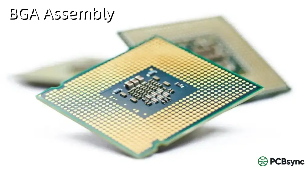
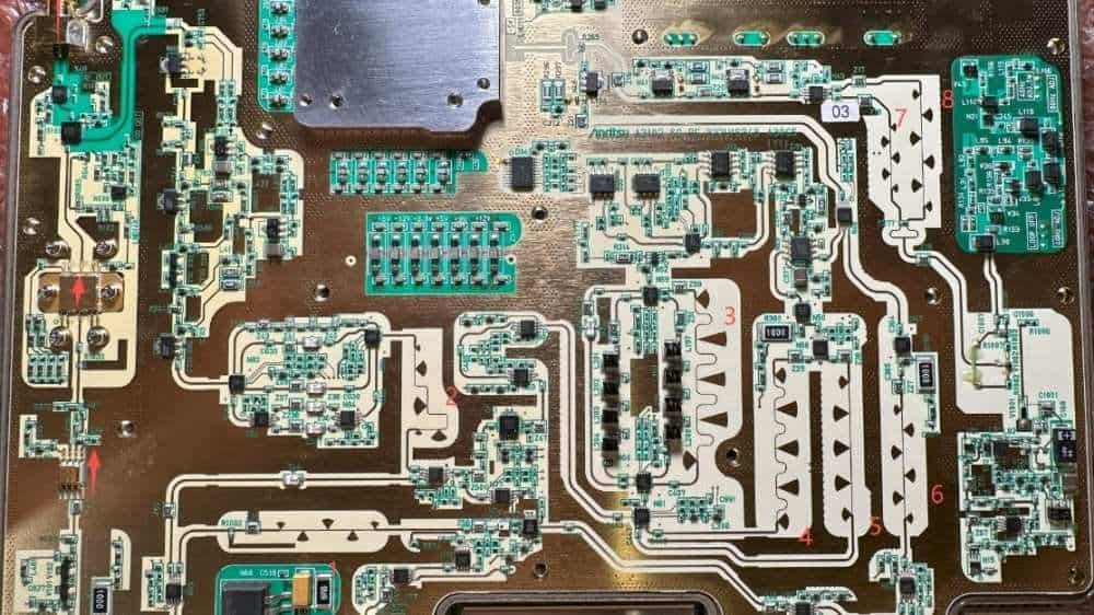
After spending over a decade working on high-density PCB projects, I can tell you that BGA assembly is one of those processes that separates amateur shops from professional manufacturers. When you’re dealing with hundreds or even thousands of tiny solder balls hidden underneath a package, there’s simply no room for guesswork.
Ball Grid Array technology has fundamentally changed how we approach high-performance electronics. Unlike traditional leaded packages where you can visually inspect every joint, BGA assembly demands precision equipment, rigorous process control, and advanced inspection methods. Get it wrong, and you’re looking at expensive rework or scrapped boards.
This guide covers everything you need to know about BGA assembly—from understanding the technology to implementing quality controls that actually work. Whether you’re an engineer specifying a new design or a production manager optimizing your SMT line, you’ll find practical, actionable information here.
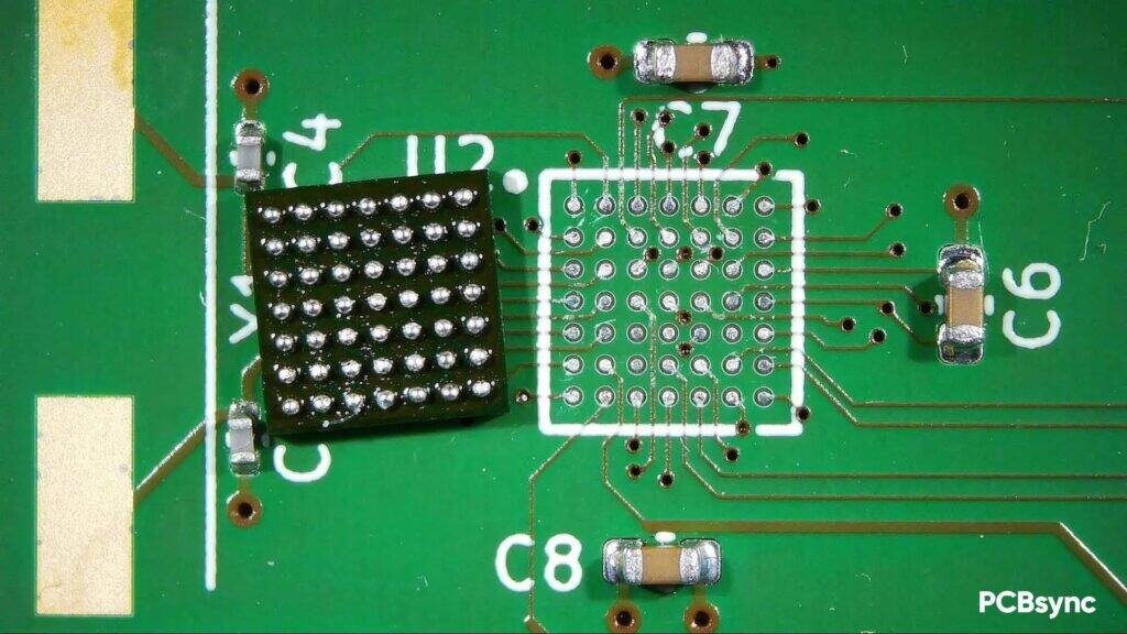
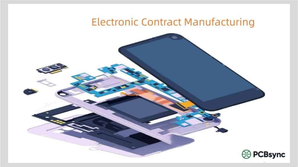
BGA assembly is the process of mounting Ball Grid Array packages onto printed circuit boards using solder reflow technology. Instead of peripheral leads like you’d find on QFP or SOIC packages, BGAs use an array of solder balls arranged in a grid pattern on the package underside. These balls serve as both the electrical connection and mechanical attachment to the PCB.
The technology emerged in the 1990s as a solution to the pin count problem. Traditional packages were running out of room around their perimeters, but BGAs could pack hundreds—even thousands—of connections into the same footprint by using the entire bottom surface. Today, you’ll find BGAs in everything from smartphones to medical devices to automotive control units.
Why BGA Over Traditional Packages?
I’ve worked with plenty of engineers who were initially skeptical about BGAs. The inspection challenges alone can seem daunting. But once you understand the advantages, the trade-offs make sense:
Higher I/O density: BGAs can accommodate 200-1000+ connections in a compact footprint. Try doing that with a QFP.
Better electrical performance: Shorter trace lengths between the die and PCB reduce inductance and improve signal integrity at high frequencies.
Improved thermal dissipation: The array of solder balls provides multiple heat paths to the PCB, reducing thermal resistance significantly.
Self-alignment during reflow: Surface tension of molten solder actually corrects minor placement errors—a nice bonus you don’t get with leaded packages.
No bent leads: Solid solder balls don’t suffer from the handling damage that plagues fine-pitch QFPs.
Types of BGA Packages
Not all BGAs are created equal. Selecting the right package type for your application requires understanding the trade-offs between cost, thermal performance, and reliability. Here’s a breakdown of the main types you’ll encounter:
Pro tip: PBGA handles most general-purpose applications cost-effectively. Reserve CBGA for environments where thermal cycling or vibration is severe.
The BGA Assembly Process: Step-by-Step
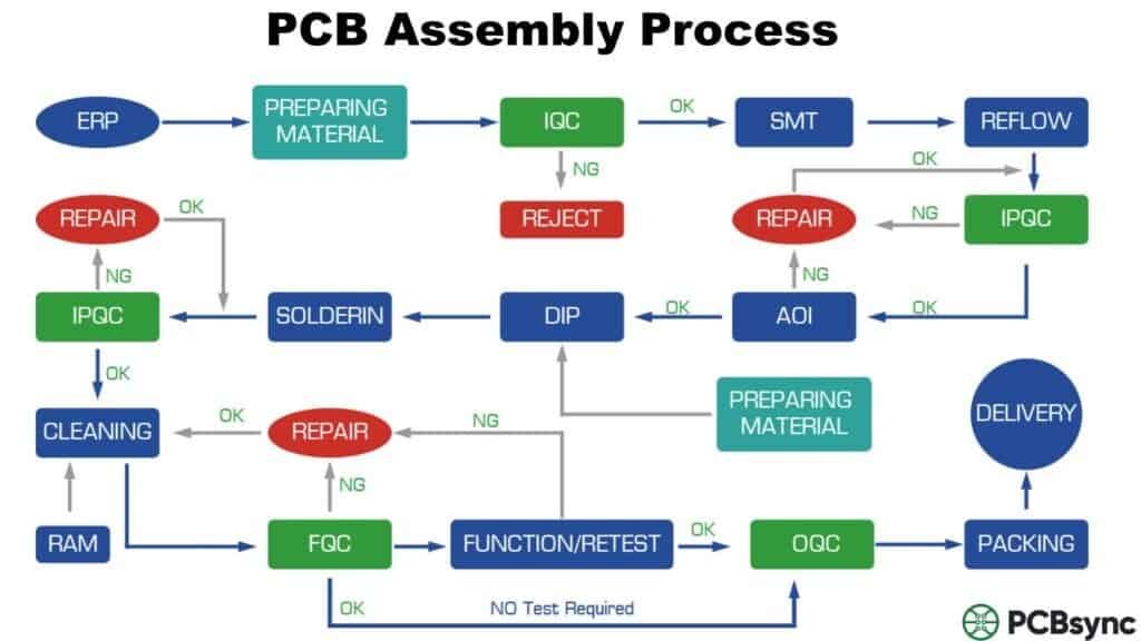
BGA assembly follows the standard SMT reflow process, but with tighter tolerances at every step. Here’s how we approach it in production:
Step 1: Solder Paste Application
This is where 50% of BGA defects originate—I’m not exaggerating. Solder paste printing determines whether your joints will form correctly during reflow.
Stencil thickness: 100-150μm for most BGAs. Fine-pitch (<0.5mm) typically uses 100μm.
Aperture design: Circular apertures for round pads. Aim for 1:1 aperture-to-pad ratio, or slightly reduced (90%) for fine pitch.
Paste type: SAC305 (Sn96.5Ag3Cu0.5) is standard for lead-free. Type 4 or Type 5 powder for fine-pitch applications.
Solder Paste Inspection (SPI): Non-negotiable. Measure paste volume, height, and area on 100% of BGA pads.
Step 2: Component Placement
Modern pick-and-place machines with vision systems can achieve ±25μm placement accuracy—essential for fine-pitch BGAs. The machine uses fiducial marks on both the component and PCB to align placement precisely.
One thing I always stress to operators: verify component orientation before running production. A rotated BGA is one of the most expensive mistakes you can make, and it’s entirely preventable.
Step 3: Reflow Soldering
The reflow profile is critical. You need enough heat to fully melt the solder balls and paste, but not so much that you damage the package or PCB. A typical SAC305 profile looks like this:
Zone
Temperature
Duration
Purpose
Preheat
150-200°C
60-90 seconds
Gradual heating, flux activation
Soak
150-200°C
90-120 seconds
Temperature equalization
Reflow
Peak: 235-250°C
60-90 seconds above 217°C
Solder melting and wetting
Cooling
< 6°C/second
Controlled descent
Joint solidification
Step 4: Inspection and Testing
Here’s the reality check: you cannot visually inspect BGA solder joints. They’re hidden underneath the package. This is where X-ray inspection becomes essential—not optional, essential.
Automated X-ray Inspection (AXI) systems can examine joint shape, detect voids, identify bridging, and verify ball placement. According to IPC-A-610 standards, voiding below 25% of the solder joint area is generally acceptable for most applications.
Common BGA Assembly Defects and How to Prevent Them
In my experience, most BGA failures trace back to process issues, not component problems. Here are the defects I see most often and how to address them:
Defect
Cause
Detection
Prevention
Voiding
Trapped flux gases, moisture in paste
X-ray inspection
Extend soak phase to 90-120s
Bridging
Excess solder paste, misalignment
X-ray, electrical test
Optimize stencil apertures
Head-in-Pillow
Oxidation, warpage, insufficient paste
X-ray (difficult to detect)
Nitrogen atmosphere, fresh paste
Open Joints
Insufficient paste, poor wetting
X-ray, ICT, functional test
Verify paste volume with SPI
Misalignment
Pick-and-place error, fiducial issues
X-ray, AOI (perimeter)
Calibrate placement, check fiducials
Quality Control and Inspection Methods
Effective BGA quality control requires a multi-layered approach. No single inspection method catches everything. Here’s the inspection strategy I recommend:
Solder Paste Inspection (SPI)
Run 100% SPI on all BGA pads before placement. Modern SPI systems measure paste volume, height, area, and position. Set limits based on your process capability—typically ±15% volume deviation is acceptable.
Automated X-ray Inspection (AXI)
This is your primary inspection method for BGA solder joints. 2D X-ray works for basic defect detection, but 3D (tomographic) systems provide much better void measurement and defect localization. According to IPC-7095, void rates below 25% of the inspection area are generally acceptable for collapsing ball BGAs.
Electrical Testing
In-Circuit Test (ICT) and functional testing catch electrical failures but can’t identify marginal joints that might fail in the field. Use electrical testing as a complement to X-ray, not a replacement.
PCB Design Considerations for BGA Assembly
Good BGA assembly starts with good PCB design. Here are the critical factors I always review:
Pad Design: NSMD vs. SMD
Non-Solder Mask Defined (NSMD) pads are preferred for BGA assembly because they provide better thermal fatigue life. The copper pad extends beyond the solder mask opening, allowing the solder joint to wrap around the pad edge. Use SMD pads only when drop/shock resistance is your primary concern.
Via Strategies
Dog-bone routing: Works well for pitches >0.65mm. Route a short trace from the pad to a via outside the BGA footprint.
Via-in-pad: Required for fine-pitch (<0.5mm) BGAs. Vias must be filled and planarized to prevent solder wicking.
Thermal vias: Place staggered arrays of thermal vias under the BGA for high-power devices.
Fiducial Marks
Always include local fiducial marks at opposite corners of BGA components. These enable precise placement alignment. The pick-and-place machine uses these marks in combination with global board fiducials for optimal accuracy.
BGA Rework and Reballing
Sometimes rework is unavoidable—defective components, engineering changes, or field failures. BGA rework requires specialized equipment and trained operators.
Basic rework process:
Preheat the board from below to minimize thermal stress.
Apply localized heat from above using IR or hot air.
Remove the BGA with a vacuum tool when solder reaches melting point.
Clean residual solder from pads using solder wick or specialized tools.
Apply fresh solder paste and place the new component.
Reflow using a controlled profile.
Inspect with X-ray to verify joint quality.
Important: Limit rework cycles to two attempts. Beyond that, you risk damaging PCB pads and degrading board reliability. IPC-7711/7721 provides detailed rework procedures.
Industry Standards and Resources
Understanding and following industry standards is crucial for consistent BGA assembly quality. Here are the key documents you should have in your library:
Standard
Description
Application
IPC-7095E
Design and Assembly Process Guidance for BGAs
Design, Assembly
IPC-A-610G
Acceptability of Electronic Assemblies
Inspection Criteria
IPC-7711/7721
Rework, Modification and Repair of Electronic Assemblies
Rework Procedures
J-STD-020
Moisture/Reflow Sensitivity Classification
Component Handling
JEDEC JEP95
Design Guide for BGA Package Standards
Package Design
Useful Resources and Downloads
Here are some resources I’ve found valuable for BGA assembly work:
IPC Standards: shop.ipc.org — Official source for IPC-7095, IPC-A-610, and other standards
Solder Paste Technical Data: Check your paste supplier’s website for specific handling and storage requirements
Component Datasheets: Always reference the component manufacturer’s recommended land patterns and reflow profiles
Industry Applications
BGA assembly is now standard across virtually every high-performance electronics sector:
Consumer Electronics: Smartphones, tablets, laptops, gaming consoles—anywhere space and performance matter.
Automotive: Engine control units, ADAS systems, infotainment. Automotive BGAs must meet stringent reliability requirements (AEC-Q100 qualification).
Medical Devices: Implantables, diagnostic equipment, patient monitoring systems. FDA Class II and III devices often require BGA technology.
Aerospace & Defense: Avionics, radar systems, satellite communications. Ceramic BGAs (CBGA) are common in these applications for their reliability.
Telecommunications: 5G infrastructure, network switches, base stations. High-speed signal integrity is critical.
Data Centers: Servers, storage systems, networking equipment. FC-BGA packages dominate in high-performance processors.
Frequently Asked Questions
1. Can I inspect BGA solder joints without X-ray equipment?
Not reliably. Visual inspection only works for the outer perimeter of balls, and even then, you can’t see the actual solder joint interface. Electrical testing can detect opens and shorts but won’t identify marginal joints or voiding. For production BGA assembly, X-ray inspection is essential—there’s really no substitute.
2. What’s the acceptable void level for BGA solder joints?
According to IPC-A-610G, voiding up to 25% of the solder joint inspection area is acceptable for Class 2 and Class 3 assemblies using collapsing (eutectic) solder balls. However, your specific application might have tighter requirements—aerospace and medical often specify lower limits. The key is documenting your acceptance criteria and validating them through reliability testing.
3. How do I handle moisture-sensitive BGA components?
Follow J-STD-020 guidelines for moisture sensitivity level (MSL) handling. Most BGAs are MSL 3 or higher, meaning they need baking before assembly if exposed to ambient conditions beyond their floor life. Store unopened components in moisture barrier bags with desiccant. Once opened, track floor life and bake at 125°C for 24+ hours if needed before reflow.
4. What causes head-in-pillow defects, and how do I prevent them?
Head-in-pillow (HiP) occurs when the solder ball and paste fail to coalesce during reflow—they touch but don’t merge. Common causes include BGA or PCB warpage, surface oxidation, and insufficient reflow peak temperature or time. Prevention strategies include using nitrogen atmosphere during reflow, ensuring fresh solder paste (check expiration), and validating your reflow profile with thermocouples on actual assemblies.
5. When should I use via-in-pad vs. dog-bone routing for BGAs?
For pitch ≥0.65mm, dog-bone routing is usually sufficient and less expensive since it doesn’t require filled and planarized vias. For fine-pitch BGAs (<0.5mm), via-in-pad becomes necessary because there’s simply not enough room between pads for escape routing. Just remember: via-in-pad requires filled and capped vias—unfilled vias will cause solder wicking and open joints.
Final Thoughts
BGA assembly isn’t inherently more difficult than other SMT processes—it just demands more precision and better process control. The fundamentals remain the same: good design, quality materials, controlled processes, and thorough inspection.
What separates successful BGA assembly from problematic production is attention to detail at every step. Invest in proper SPI and AXI equipment. Train your operators on moisture sensitivity handling. Validate your reflow profiles with actual product, not just test boards. And document everything—when something goes wrong, you’ll want that data.
The payoff is worth it. BGAs enable designs that simply aren’t possible with traditional packages—higher performance, smaller footprints, better thermal management. Master the process, and you’ll have a competitive advantage that’s hard for others to match.
Have questions about BGA assembly for your specific application? The comments section below is open, and I’m always happy to discuss real-world challenges.
Inquire: Call 0086-755-23203480, or reach out via the form below/your sales contact to discuss our design, manufacturing, and assembly capabilities.
Quote: Email your PCB files to Sales@pcbsync.com (Preferred for large files) or submit online. We will contact you promptly. Please ensure your email is correct.
Notes: For PCB fabrication, we require PCB design file in Gerber RS-274X format (most preferred), *.PCB/DDB (Protel, inform your program version) format or *.BRD (Eagle) format. For PCB assembly, we require PCB design file in above mentioned format, drilling file and BOM. Click to download BOM template To avoid file missing, please include all files into one folder and compress it into .zip or .rar format.


