Inquire: Call 0086-755-23203480, or reach out via the form below/your sales contact to discuss our design, manufacturing, and assembly capabilities.
Quote: Email your PCB files to Sales@pcbsync.com (Preferred for large files) or submit online. We will contact you promptly. Please ensure your email is correct.
Notes: For PCB fabrication, we require PCB design file in Gerber RS-274X format (most preferred), *.PCB/DDB (Protel, inform your program version) format or *.BRD (Eagle) format. For PCB assembly, we require PCB design file in above mentioned format, drilling file and BOM. Click to download BOM template To avoid file missing, please include all files into one folder and compress it into .zip or .rar format.
After spending over a decade in PCB manufacturing, I’ve seen countless boards fail in the field because of issues that could have been caught during testing. The bed of nails test remains one of the most reliable methods we use to catch these defects before they become expensive problems. If you’re involved in electronics manufacturing or quality control, understanding this testing method isn’t optional—it’s essential.
In this comprehensive guide, I’ll walk you through everything you need to know about bed of nails testing, from basic concepts to advanced implementation strategies. Whether you’re designing PCBs, managing a production line, or evaluating testing options for your next project, this information will help you make informed decisions.
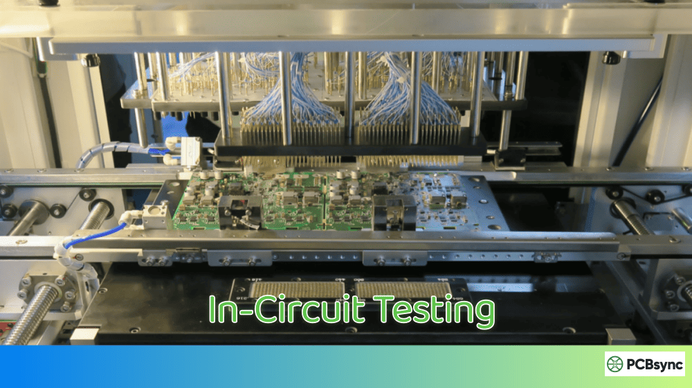
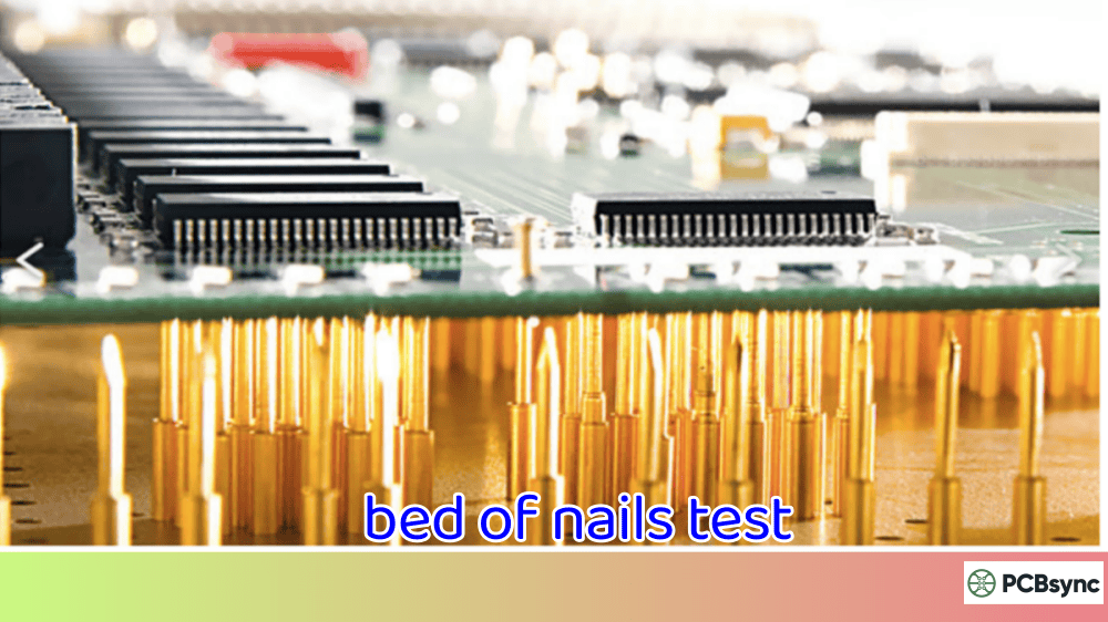
A bed of nails test is a traditional electronic test fixture used for In-Circuit Testing (ICT) of printed circuit boards. The name comes from its physical appearance—an array of spring-loaded pins (called pogo pins) protruding from a flat surface, resembling the classic bed of nails you might have seen in magic shows.
These pins are precisely aligned with test points on your PCB design. When the board is pressed down against the fixture, hundreds or even thousands of individual connections are made simultaneously. This allows the testing equipment to check electrical continuity, measure component values, and verify that your board matches its intended design—all in a matter of seconds.
The bed of nails test fixture works with an in-circuit tester to perform electrical measurements. The fixture itself consists of several key components: a G-10 laminated base plate, spring-loaded pogo pins, tooling pins for alignment, and wiring connections to the measurement unit. Each pogo pin makes contact with a specific node in your circuit, creating a complete electrical map of the board.
How Does Bed of Nails Testing Work?
The bed of nails testing process follows a straightforward but precise sequence. Understanding this workflow helps you appreciate why proper test point design matters so much during the PCB layout phase.
The Testing Process Step by Step
Fixture Design and Manufacturing: A custom fixture is created based on your PCB’s test point locations. This typically takes 4-6 weeks and involves precision drilling of pin holes in the G-10 plate.
Board Loading: The PCB (now called the Device Under Test or DUT) is placed on the fixture using tooling pins for precise alignment.
Contact Application: The board is pressed down onto the bed of nails using either vacuum force (100-200 grams per pin) or mechanical pressure. This ensures reliable electrical contact at all test points.
Electrical Testing: The ICT equipment applies test signals through the pogo pins and measures responses, checking for shorts, opens, and component values.
Results Analysis: The tester compares measured values against the reference netlist and generates a pass/fail report, often identifying specific fault locations.
Types of Bed of Nails Fixtures
Not all bed of nails fixtures are created equal. The type you choose depends on your production volume, board complexity, and budget constraints.
Vacuum Fixtures: Use vacuum pressure to pull the PCB down onto the pins. They provide more consistent contact and better signal readings but cost more and aren’t suitable for automated production lines.
Press-Down Fixtures: Use mechanical force from above to press the board onto the pins. More economical and compatible with automated handlers, but may have slightly less consistent contact pressure.
Clamshell Fixtures: Feature hinged top and bottom plates with pogo pins, allowing access to both sides of the PCB. Ideal for double-sided boards with test points on both surfaces.
Hybrid Fixtures: Combine fixed bed of nails with movable flying probes to access difficult test nodes that fixed pins can’t reach.
What Defects Does Bed of Nails Testing Detect?
One of the biggest advantages of bed of nails testing is its comprehensive defect coverage. The method can identify a wide range of manufacturing issues that would be impossible to catch with visual inspection alone.
Table 1: Manufacturing Defects Detected by Bed of Nails Testing
Defect Type
Description
Detection Method
Short Circuits
Unintended connections between separate nets
Isolation resistance testing
Open Circuits
Broken traces, incomplete etching, damaged vias
Continuity testing
Wrong Component Values
Incorrect resistor, capacitor, or inductor values
Component measurement
Missing Components
Components not placed during assembly
Presence verification
Reversed Polarity
Diodes, capacitors, or ICs installed backwards
Polarity testing
Solder Bridges
Excess solder connecting adjacent pins
Isolation testing between pins
Cold Solder Joints
Poor solder connections with high resistance
Resistance threshold comparison
Bed of Nails Test vs Flying Probe Testing: Which Should You Choose?
This is probably the question I get asked most often. Both methods have their place, and the right choice depends entirely on your specific situation. Let me break down the key differences from a practical engineering perspective.
Table 2: Bed of Nails Test vs Flying Probe Comparison
Factor
Bed of Nails (ICT)
Flying Probe
Test Speed
5-15 seconds per board
1-15 minutes per board
Fixture Cost
$5,000 – $50,000+ per design
No custom fixture required
Setup Time
4-6 weeks for fixture fabrication
Hours to program
Test Coverage
90-100% with proper DFT
70-85% on complex boards
Best For
High-volume production (1,000+ units)
Prototypes and low-volume runs
Design Flexibility
Requires fixture rebuild for changes
Software update only
Per-Unit Cost
Low after fixture amortization
Higher due to test time
Here’s my rule of thumb: if you’re producing fewer than 500 units or expect frequent design changes, flying probe is usually more economical. For anything over 1,000 units with a stable design, bed of nails testing typically offers the best return on investment.
Design for Testability: Getting Your PCB Ready for Bed of Nails Testing
I’ve seen too many PCB designs that look great on paper but become nightmares when it’s time for testing. Following these DFT guidelines during layout will save you significant headaches—and money—down the road.
Test Point Design Specifications
Table 3: Test Point Design Requirements
Parameter
Recommended Value
Test Pad Diameter (Standard)
0.035″ (0.9mm) nominal, 0.015″-0.040″ range
Minimum Pad Spacing
0.100″ (2.54mm) preferred, 0.050″ minimum
Clearance from Board Edge
0.125″ (3.2mm) minimum
Clearance from Components
0.040″ (1mm) minimum from SMD components
Tooling Hole Diameter
0.125″ (3.2mm) unplated, ±0.002″ tolerance
Probe Density Limit
12 probes per square inch maximum
Grid Spacing (Fine Pitch)
0.8mm minimum for small probes
Essential DFT Best Practices
Place test points on the solder side: For SMT boards, always use dedicated test pads rather than probing component leads directly. Probing leads can create temporary connections that mask real defects.
Provide test access to all nets: Every signal net should have at least one accessible test point. Include multiple points for power and ground planes to ensure even distribution during testing.
Use unplated tooling holes: Place two or three diagonally opposed tooling holes for alignment. Keep them unplated to avoid solder contamination and maintain tight tolerances.
Avoid test points under tall components: Components over 0.35″ tall require milling the test fixture for clearance. Place test points at least 0.1″ away from such components.
Make control signals accessible: Reset lines, clock inputs, and enable signals should all be testable. Don’t tie them directly to VCC or ground through common resistors.
If you’re working in aerospace, medical, automotive, or military applications, compliance with industry standards isn’t optional. The primary standard governing PCB electrical testing is IPC-9252B—Requirements for Electrical Testing of Unpopulated Printed Boards.
IPC Classification Requirements
Table 4: IPC-9252 Classification Requirements
IPC Class
Application
Test Requirements
Class 1
General electronics (consumer products, toys)
Basic continuity/isolation
Class 2
Dedicated service (industrial, telecom, computers)
100% netlist verification
Class 3
High reliability (medical, military, aerospace)
HiPot, strict thresholds
Class 3/A
Aerospace and military avionics
250VDC, 100MΩ isolation
For Class 3 applications, the standard specifies continuity resistance must be below 10 ohms, and isolation resistance between separate nets must exceed 10 megohms. Class 3/A has even stricter requirements: 250VDC test voltage and 100 megohm isolation threshold.
Advantages and Limitations of Bed of Nails Testing
Let me give you an honest assessment based on real-world experience. Bed of nails testing is powerful, but it’s not perfect for every situation.
Key Advantages
Speed: Testing a board in under 10 seconds makes it ideal for high-volume production lines where throughput matters.
Comprehensive coverage: With proper DFT, you can achieve 90%+ test coverage, catching defects that would slip through other methods.
Repeatability: Once calibrated, the fixture produces consistent results across thousands of boards.
Automated operation: Minimal operator intervention required after setup, reducing labor costs and human error.
Early defect detection: Catching issues before final pcb assembly saves significant rework costs.
Known Limitations
High fixture cost: Custom fixtures can cost $5,000-$50,000+ depending on complexity, making them impractical for low-volume runs.
Long lead time: 4-6 weeks to design and manufacture a fixture doesn’t work for rapid prototyping.
Design inflexibility: Moving a test point by just 0.05″ can make the entire fixture obsolete.
Potential mechanical damage: Excessive board flexure can cause capacitor cracking or pad cratering if support placement isn’t optimized.
Access challenges: Dense SMT boards with components on both sides can create node access difficulties.
Cost Analysis: When Does Bed of Nails Testing Make Financial Sense?
Let’s talk numbers. I’ve helped many clients work through this calculation, and the break-even point varies significantly based on your specific circumstances.
Table 5: Cost Comparison Example (10,000 Unit Run)
Cost Factor
Bed of Nails vs Flying Probe
Fixture/Setup Cost
$20,000 (BON) vs $500 programming (FP)
Test Time per Board
10 seconds (BON) vs 5 minutes (FP)
Machine Time Cost (10K units)
$833 (BON) vs $25,000 (FP)
Total Testing Cost
$20,833 (BON) vs $25,500 (FP)
Cost per Board
$2.08 (BON) vs $2.55 (FP)
In this example, bed of nails testing becomes more economical around 4,000-5,000 units. Your actual break-even point depends on fixture complexity, machine rates, and how much your design might change during production.
Useful Resources and Further Reading
Here are some valuable resources I recommend for engineers working with bed of nails testing:
IPC-9252B Standard: Requirements for Electrical Testing of Unpopulated Printed Boards – https://shop.ipc.org
IPC-D-356 Format Specification: Bare Substrate Electrical Test Point Data Description – essential for test programming
IPC-TM-650: Test Methods Manual – includes dielectric withstanding voltage and other electrical test procedures
SPEA Test Equipment Resources: Flying probe and ICT technical documentation – https://www.spea.com
Frequently Asked Questions About Bed of Nails Testing
How long does it take to develop a bed of nails test fixture?
Typically 4-6 weeks from design file submission to completed fixture. This includes fixture design, G-10 plate drilling, pogo pin installation, wiring, and programming. Complex boards with high pin counts may take longer. Some manufacturers offer expedited services for 2-3 week turnaround at additional cost.
Can bed of nails testing damage my PCB?
When properly designed, the risk is minimal. However, excessive board flexure from poor support placement or high probe forces can cause capacitor flex cracking and pad cratering. You may notice small dimples from pogo pin contact—this is normal and doesn’t affect functionality. Always ensure your fixture manufacturer optimizes support locations and probe forces for your specific board.
What’s the minimum production volume where bed of nails testing makes sense?
The break-even point is typically between 500-1,000 units, depending on board complexity and fixture cost. For medical, aerospace, or military applications where IPC Class 3 testing is required, bed of nails may be necessary regardless of volume due to coverage requirements. For prototype and low-volume work, flying probe testing is usually more economical.
How often do pogo pins need replacement?
Quality pogo pins typically last 100,000-500,000 cycles depending on construction and maintenance. Schedule regular cleaning to remove flux residue and inspect for wear. Signs that pins need replacement include intermittent contact failures, inconsistent readings, and visible tip damage. Budget for pin replacement as an ongoing maintenance cost, especially in high-volume production.
Can I test SMT boards with bed of nails fixtures?
Yes, but you must design dedicated test pads into your PCB layout. Never probe SMT component leads directly—the probe pressure can temporarily connect open solder joints, masking real defects, or damage fine-pitch leads. Test pads should be at least 0.035″ diameter with 0.050″ minimum spacing. Position them on the bottom side of the board for best fixture access.
Conclusion: Is Bed of Nails Testing Right for Your Project?
The bed of nails test remains one of the most reliable and efficient methods for PCB quality control in high-volume manufacturing. Its ability to simultaneously test hundreds of points, detect a comprehensive range of defects, and deliver results in seconds makes it indispensable for production environments where quality and throughput both matter.
However, it’s not the right solution for every situation. If you’re working on prototypes, expecting design changes, or producing fewer than 500 units, flying probe testing likely offers better value. The key is matching your testing strategy to your specific production requirements.
Remember: the best time to plan for testability is during PCB layout, not after you’ve already sent files for fabrication. Incorporate the DFT guidelines I’ve outlined, work with your test fixture manufacturer early in the design process, and you’ll avoid the costly redesigns that plague engineers who treat testing as an afterthought.
Whether you choose bed of nails, flying probe, or a combination of both, the goal is the same: catching defects before they become expensive field failures. That’s what quality testing is all about.
Inquire: Call 0086-755-23203480, or reach out via the form below/your sales contact to discuss our design, manufacturing, and assembly capabilities.
Quote: Email your PCB files to Sales@pcbsync.com (Preferred for large files) or submit online. We will contact you promptly. Please ensure your email is correct.
Notes: For PCB fabrication, we require PCB design file in Gerber RS-274X format (most preferred), *.PCB/DDB (Protel, inform your program version) format or *.BRD (Eagle) format. For PCB assembly, we require PCB design file in above mentioned format, drilling file and BOM. Click to download BOM template To avoid file missing, please include all files into one folder and compress it into .zip or .rar format.


