Inquire: Call 0086-755-23203480, or reach out via the form below/your sales contact to discuss our design, manufacturing, and assembly capabilities.
Quote: Email your PCB files to Sales@pcbsync.com (Preferred for large files) or submit online. We will contact you promptly. Please ensure your email is correct.
Notes: For PCB fabrication, we require PCB design file in Gerber RS-274X format (most preferred), *.PCB/DDB (Protel, inform your program version) format or *.BRD (Eagle) format. For PCB assembly, we require PCB design file in above mentioned format, drilling file and BOM. Click to download BOM template To avoid file missing, please include all files into one folder and compress it into .zip or .rar format.
If you’ve ever programmed an Arduino Uno, you’ve already worked with the ATmega328P—even if you didn’t realize it. This 8-bit microcontroller sits at the heart of countless development boards and commercial products, from simple LED blinkers to sophisticated industrial control systems.
After designing dozens of boards around this chip, I’ve developed a deep appreciation for what Microchip (formerly Atmel) packed into this unassuming 28-pin package. This guide breaks down the ATmega328P datasheet into practical knowledge you can actually use, whether you’re building your first custom PCB or optimizing an existing design.
The ATmega328P is an 8-bit CMOS microcontroller based on the AVR enhanced RISC architecture. That’s a mouthful, so let’s unpack it:
8-bit means the processor handles data in 8-bit chunks. While this limits raw computational power compared to 32-bit ARM processors, it’s more than sufficient for most embedded applications—and the simplicity translates to lower power consumption and easier debugging.
RISC (Reduced Instruction Set Computer) architecture means the ATmega328P executes most instructions in a single clock cycle. The processor includes 131 instructions, with 32 general-purpose working registers directly connected to the Arithmetic Logic Unit (ALU). This design achieves throughputs approaching 1 MIPS per MHz.
The “P” suffix indicates “picoPower” technology—Microchip’s branding for enhanced power-saving features including multiple sleep modes.
ATmega328P Technical Specifications Summary
Before diving deeper, here’s a quick reference of the core specifications every designer needs:
Parameter
Specification
Architecture
8-bit AVR RISC
Operating Voltage
1.8V – 5.5V
Maximum Clock Frequency
20 MHz (at 4.5V-5.5V)
Flash Memory (Program)
32 KB (with 0.5KB bootloader section)
SRAM (Data)
2 KB
EEPROM
1 KB
GPIO Pins
23
ADC Channels
6 (10-bit resolution)
PWM Channels
6
Timers
2× 8-bit, 1× 16-bit
Communication
USART, SPI, I2C (TWI)
Operating Temperature
-40°C to +85°C (industrial)
These specifications explain why the ATmega328P became the de facto standard for entry-level embedded development. The memory is generous enough for substantial programs, the I/O count handles most sensor interfaces, and the operating voltage range accommodates both 3.3V and 5V systems.
ATmega328P Architecture and Block Diagram
Understanding the ATmega328P’s internal architecture helps when optimizing code or troubleshooting timing issues.
CPU Core and Register File
The ATmega328P uses a modified Harvard architecture with separate buses for program memory (Flash) and data memory (SRAM). This allows simultaneous instruction fetch and data access—a key factor in achieving single-cycle execution for most instructions.
The 32 general-purpose registers (R0-R31) connect directly to the ALU. Two registers can be accessed during a single clock cycle, enabling true single-cycle operations. Six of these registers (R26-R31) can function as 16-bit pointer registers for indirect addressing—essential for efficient array and structure manipulation.
Memory Organization
The ATmega328P organizes memory into three distinct spaces:
Memory Type
Size
Address Range
Endurance
Purpose
Flash
32 KB
0x0000 – 0x3FFF
10,000 cycles
Program storage
SRAM
2 KB
0x0100 – 0x08FF
Unlimited
Runtime variables
EEPROM
1 KB
0x0000 – 0x03FF
100,000 cycles
Non-volatile data
Flash memory stores your compiled program. The 32KB capacity sounds limited by modern standards, but AVR code is remarkably compact. Most Arduino sketches use only a fraction of available space.
SRAM holds variables, the stack, and the heap during program execution. The 2KB allocation requires careful management in memory-intensive applications—a common source of mysterious crashes when variables overflow into the stack.
EEPROM provides persistent storage for configuration parameters, calibration data, or operational logs. The 100,000 write cycle endurance means you can write once per second for over three years before wear becomes a concern.
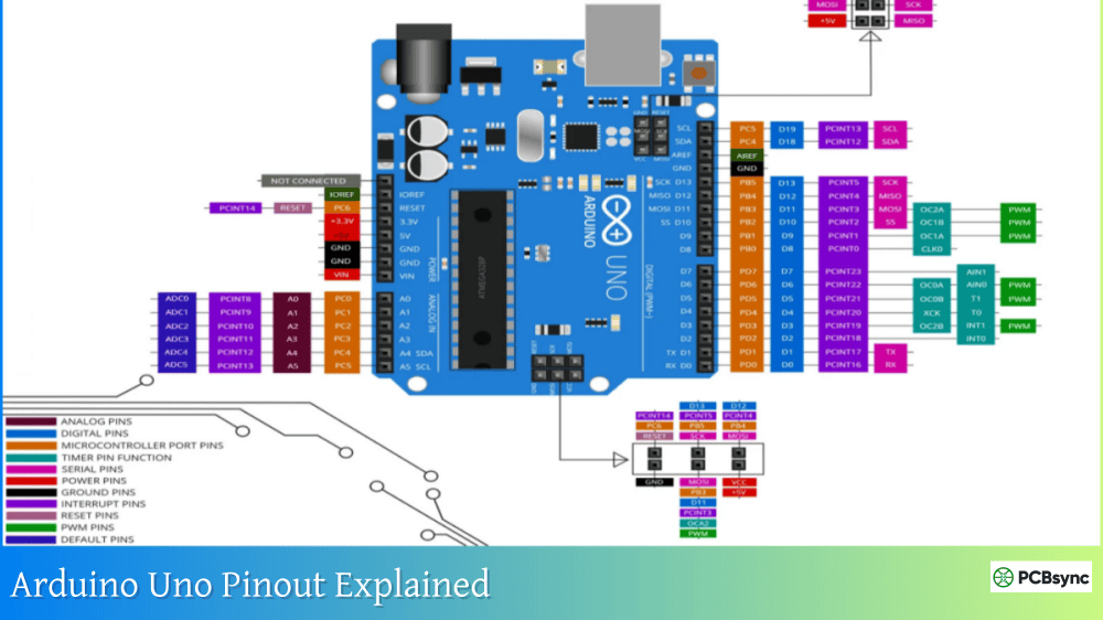
ATmega328P Pinout and Pin Configuration
The ATmega328P comes in four package options: 28-pin PDIP, 28-pin TQFP, 32-pin TQFP, and 32-pin VQFN. The PDIP version remains popular for prototyping and through-hole designs, while the TQFP and VQFN packages suit production PCBs where space matters.
ATmega328P Pin Functions Table
Pin (PDIP)
Port
Primary Function
Alternate Functions
1
PC6
RESET
PCINT14
2
PD0
Digital I/O
RXD (USART), PCINT16
3
PD1
Digital I/O
TXD (USART), PCINT17
4
PD2
Digital I/O
INT0, PCINT18
5
PD3
Digital I/O
INT1, OC2B (PWM), PCINT19
6
PD4
Digital I/O
T0, XCK, PCINT20
7
VCC
Power Supply
—
8
GND
Ground
—
9
PB6
Crystal
XTAL1, TOSC1, PCINT6
10
PB7
Crystal
XTAL2, TOSC2, PCINT7
11
PD5
Digital I/O
T1, OC0B (PWM), PCINT21
12
PD6
Digital I/O
AIN0, OC0A (PWM), PCINT22
13
PD7
Digital I/O
AIN1, PCINT23
14
PB0
Digital I/O
ICP1, CLKO, PCINT0
15
PB1
Digital I/O
OC1A (PWM), PCINT1
16
PB2
Digital I/O
SS (SPI), OC1B (PWM), PCINT2
17
PB3
Digital I/O
MOSI (SPI), OC2A (PWM), PCINT3
18
PB4
Digital I/O
MISO (SPI), PCINT4
19
PB5
Digital I/O
SCK (SPI), PCINT5
20
AVCC
ADC Power
—
21
AREF
ADC Reference
—
22
GND
Ground
—
23
PC0
ADC0
PCINT8
24
PC1
ADC1
PCINT9
25
PC2
ADC2
PCINT10
26
PC3
ADC3
PCINT11
27
PC4
ADC4
SDA (I2C), PCINT12
28
PC5
ADC5
SCL (I2C), PCINT13
Critical Pin Considerations for PCB Design
AVCC (Pin 20) must be connected to VCC through a low-pass filter, even if you’re not using the ADC. I typically use a 10µH inductor with 100nF bypass capacitor. Leaving AVCC floating causes unpredictable behavior.
AREF (Pin 21) should have a 100nF decoupling capacitor to ground for noise rejection when using the internal reference. If using an external reference, connect your precision voltage source here.
Reset (Pin 1) needs proper external circuitry: a 10kΩ pull-up resistor to VCC and optionally a 100nF capacitor to ground for noise immunity. The reset threshold is approximately 0.2×VCC to 0.9×VCC.
Crystal Pins (PB6/PB7) require load capacitors calculated based on crystal specifications. For a typical 16MHz crystal with 20pF load capacitance, use two 22pF capacitors (accounting for stray PCB capacitance).
ATmega328P Timer/Counter System
The ATmega328P includes three timer/counter modules—a versatile system that handles everything from precise delays to PWM generation to external event counting.
Timer/Counter Overview
Timer
Resolution
PWM Outputs
Special Features
Timer0
8-bit
OC0A, OC0B
Fast PWM, Phase Correct PWM
Timer1
16-bit
OC1A, OC1B
Input capture, CTC mode
Timer2
8-bit
OC2A, OC2B
Asynchronous operation (32.768kHz)
Timer0 typically handles the Arduino millis() and micros() functions. It’s configured in Fast PWM mode with a prescaler that produces overflow interrupts approximately every 1.024ms.
Timer1 is the powerhouse—16-bit resolution means you can generate PWM frequencies from sub-hertz to hundreds of kilohertz with excellent duty cycle resolution. The input capture function timestamps external events with single-clock precision.
Timer2 offers asynchronous operation from a 32.768kHz watch crystal, enabling accurate timekeeping even during sleep modes. This is how real-time clock applications maintain time while the main oscillator is stopped.
PWM Generation on ATmega328P
The ATmega328P supports multiple PWM modes:
Mode
Description
Best For
Fast PWM
Single-slope counting
LED dimming, motor speed
Phase Correct PWM
Dual-slope counting
Motor control, audio
Phase/Frequency Correct
Symmetric PWM
Precision motor control
Arduino’s analogWrite() function uses Fast PWM with an 8-bit resolution, producing approximately 490Hz or 980Hz depending on which pin you use. Direct register manipulation unlocks frequencies from DC to several hundred kilohertz.
ATmega328P Analog-to-Digital Converter (ADC)
The integrated 10-bit successive approximation ADC provides adequate resolution for most sensor interfaces.
ADC Specifications
Parameter
Value
Resolution
10 bits (1024 steps)
Channels
6 single-ended, 1 differential pair
Conversion Time
13-260µs (depending on prescaler)
Input Voltage Range
0V to VREF
Accuracy
±2 LSB absolute, ±0.5 LSB INL
ADC Reference Options
The ATmega328P offers three voltage reference sources:
Reference
Voltage
Use Case
AVCC
~5V
General purpose, ratiometric sensors
Internal
1.1V
Low-voltage precision measurements
External AREF
0V to VCC
Custom reference voltage
For battery-powered applications, the internal 1.1V reference enables monitoring the supply voltage itself—useful for low-battery warnings.
ATmega328P Communication Interfaces
The ATmega328P includes three hardware communication peripherals, covering most embedded connectivity needs.
The single USART channel supports baud rates from 2400 to 2Mbps (at 16MHz). It handles standard serial communication with computers, GPS modules, Bluetooth adapters, and other serial devices.
SPI (Serial Peripheral Interface)
The SPI module operates in master or slave mode at speeds up to half the system clock (8MHz at 16MHz system clock). SPI connects to SD cards, displays, external ADCs, and high-speed sensors.
TWI (Two-Wire Interface / I2C)
The hardware TWI module supports both master and slave modes up to 400kHz. I2C’s two-wire simplicity makes it ideal for connecting multiple sensors, EEPROMs, and low-speed peripherals.
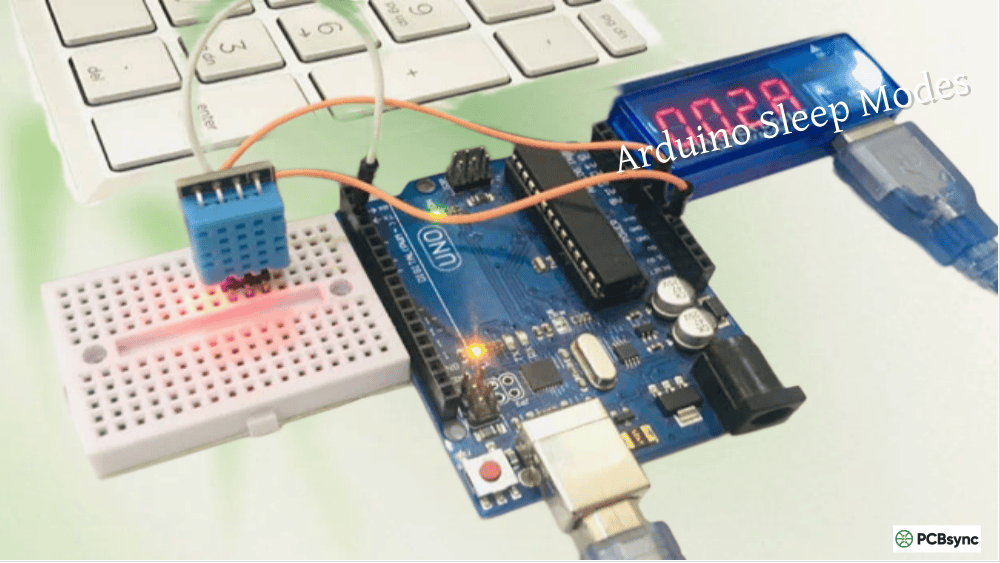
The “picoPower” technology in the ATmega328P provides six power-saving modes:
Sleep Mode
Active Components
Current Draw (typical)
Idle
CPU halted, peripherals active
~1.5mA at 8MHz
ADC Noise Reduction
ADC enabled only
~0.3mA
Power-down
32kHz oscillator only
~0.1µA
Power-save
Timer2 with 32kHz crystal
~0.75µA
Standby
Main oscillator running
~0.05mA
Extended Standby
Main + 32kHz oscillators
~0.05mA
The Power-down mode achieves the lowest consumption—essential for battery-powered applications. Combined with watchdog timer wake-up, you can create devices that run for years on coin cells.
Programming the ATmega328P
Multiple programming methods exist for the ATmega328P:
In-System Programming (ISP)
The 6-pin ISP interface (MOSI, MISO, SCK, RESET, VCC, GND) allows programming without removing the chip. Standard AVR programmers like USBasp or Arduino as ISP work reliably.
Bootloader Programming
The ATmega328P reserves 512 bytes to 4KB (configurable via fuses) for a bootloader. The Arduino bootloader enables programming over UART—the familiar method when uploading sketches.
JTAG Debugging
While the ATmega328P lacks dedicated JTAG pins, debugWIRE interface through the RESET pin enables on-chip debugging with Atmel-ICE or similar tools.
Arduino Pin Mapping to ATmega328P
Understanding how Arduino pins map to ATmega328P ports helps when reading datasheets or writing register-level code:
Arduino Pin
ATmega328P Pin
Port
Special Function
D0
2
PD0
RX
D1
3
PD1
TX
D2
4
PD2
INT0
D3
5
PD3
INT1, PWM
D4
6
PD4
—
D5
11
PD5
PWM
D6
12
PD6
PWM
D7
13
PD7
—
D8
14
PB0
—
D9
15
PB1
PWM
D10
16
PB2
PWM, SS
D11
17
PB3
PWM, MOSI
D12
18
PB4
MISO
D13
19
PB5
SCK, LED
A0
23
PC0
ADC0
A1
24
PC1
ADC1
A2
25
PC2
ADC2
A3
26
PC3
ADC3
A4
27
PC4
ADC4, SDA
A5
28
PC5
ADC5, SCL
ATmega328P Resources and Downloads
Resource
Description
Source
Complete Datasheet
442-page technical reference
Microchip website
Automotive Datasheet
AEC-Q100 qualified variant
Microchip website
AVR Instruction Set Manual
Assembly language reference
Microchip website
Arduino Bootloader
Optiboot source code
GitHub arduino/optiboot
AVR Libc Reference
C library documentation
nongnu.org/avr-libc
ATmega328P CAD Symbols
Schematic symbols and footprints
Ultra Librarian, SnapEDA
ATmega328P vs ATmega328PB: Key Differences
Microchip released the ATmega328PB as an enhanced version. Key differences include:
Feature
ATmega328P
ATmega328PB
Timers
3
5
USART
1
2
SPI
1
2
I2C
1
2
GPIO
23
27
Touch Channels
0
24 (PTC)
The ATmega328PB isn’t a drop-in replacement due to different fuse configurations and additional pins, but it offers significant capability upgrades for new designs.
Frequently Asked Questions About ATmega328P
What is the maximum clock speed of ATmega328P?
The ATmega328P runs at up to 20MHz when powered between 4.5V and 5.5V. At lower voltages (1.8V-4.5V), the maximum safe frequency drops to 10MHz. Most Arduino boards run at 16MHz, which provides adequate margin across the operating voltage range.
How much current can ATmega328P GPIO pins source or sink?
Each I/O pin can source or sink up to 40mA, with a recommended maximum of 20mA for reliable operation. The total current through VCC and GND pins combined should not exceed 200mA. For higher current loads, use external transistors or MOSFETs.
Can ATmega328P run without an external crystal?
Yes. The ATmega328P includes an internal 8MHz RC oscillator with ±10% accuracy at factory calibration. Many applications work fine with this internal clock, though UART communication becomes unreliable at high baud rates due to frequency drift with temperature.
What’s the difference between ATmega328 and ATmega328P?
The “P” variant includes picoPower technology for reduced power consumption, particularly in sleep modes. The ATmega328P draws significantly less current in Power-down mode (0.1µA vs 0.5µA typical). For new designs, always choose the ATmega328P.
How do I recover an ATmega328P with wrong fuse settings?
If you accidentally configure fuses that disable the clock source, you’ll need a high-voltage programmer (HVPP) to reset them. The STK500 or dedicated HV rescue boards can recover “bricked” chips. Always double-check fuse calculations before programming.
Conclusion: Why ATmega328P Remains Relevant
Despite newer, more powerful microcontrollers flooding the market, the ATmega328P maintains its position as the go-to chip for learning embedded systems and building reliable, cost-effective products.
The ATmega328P succeeds because it hits a sweet spot: enough capability for real-world applications, simple enough to understand thoroughly, and supported by decades of documentation, tutorials, and community knowledge. When you understand this chip’s datasheet inside and out, you’ve built a foundation that transfers to any microcontroller platform.
For hobbyists, the Arduino ecosystem makes the ATmega328P immediately accessible. For professionals, the chip’s long production history, multiple qualified sources, and automotive-grade variants ensure supply chain stability that newer parts can’t match.
Whether you’re designing your first custom PCB or optimizing a production device, investing time in understanding the ATmega328P pays dividends across your entire embedded development career.
Inquire: Call 0086-755-23203480, or reach out via the form below/your sales contact to discuss our design, manufacturing, and assembly capabilities.
Quote: Email your PCB files to Sales@pcbsync.com (Preferred for large files) or submit online. We will contact you promptly. Please ensure your email is correct.
Notes: For PCB fabrication, we require PCB design file in Gerber RS-274X format (most preferred), *.PCB/DDB (Protel, inform your program version) format or *.BRD (Eagle) format. For PCB assembly, we require PCB design file in above mentioned format, drilling file and BOM. Click to download BOM template To avoid file missing, please include all files into one folder and compress it into .zip or .rar format.


