Inquire: Call 0086-755-23203480, or reach out via the form below/your sales contact to discuss our design, manufacturing, and assembly capabilities.
Quote: Email your PCB files to Sales@pcbsync.com (Preferred for large files) or submit online. We will contact you promptly. Please ensure your email is correct.
Notes: For PCB fabrication, we require PCB design file in Gerber RS-274X format (most preferred), *.PCB/DDB (Protel, inform your program version) format or *.BRD (Eagle) format. For PCB assembly, we require PCB design file in above mentioned format, drilling file and BOM. Click to download BOM template To avoid file missing, please include all files into one folder and compress it into .zip or .rar format.
How to Convert Altium & Eagle Projects to KiCad (Step-by-Step)
If you’ve spent any time in the PCB design world, you know the frustration of dealing with projects stuck in proprietary formats. Maybe you inherited an old Eagle design from a colleague, received reference files from a vendor in Altium format, or simply want to migrate your entire library to an open-source solution. Whatever your situation, converting Altium to KiCad or Eagle to KiCad doesn’t have to be a nightmare.
I’ve been through this process dozens of times—importing TI reference designs, rescuing legacy boards from defunct Eagle installations, and helping clients move their entire portfolios to KiCad. In this guide, I’ll walk you through everything you need to know about EDA project conversion, including the native methods, third-party tools, and the gotchas that nobody tells you about until you’re knee-deep in broken netlists.
Before diving into the how, let’s briefly address the why. KiCad has transformed from a hobbyist tool into a legitimate professional PCB design suite. With the release of KiCad 7 and the substantial improvements in KiCad 8 and 9, the import capabilities have expanded dramatically.
The biggest drivers for migration include:
The discontinuation of standalone Eagle by Autodesk (scheduled sunset in 2026) has left thousands of engineers scrambling for alternatives. Altium Designer’s subscription costs can be prohibitive for small teams or independent consultants. KiCad offers unlimited board size, layer count, and schematic complexity—no artificial limitations like Eagle’s free version had.
Understanding File Formats Before Conversion
Getting familiar with the file extensions you’re dealing with saves headaches later. Here’s what you’ll encounter:
Altium Designer File Formats
File Extension
Description
KiCad Equivalent
.SchDoc
Schematic document
.kicad_sch
.PcbDoc
PCB layout file
.kicad_pcb
.PrjPcb
Project file
.kicad_pro
.SchLib
Symbol library
.kicad_sym
.PcbLib
Footprint library
.kicad_mod
.IntLib
Integrated library
.kicad_sym + .kicad_mod
Eagle File Formats
File Extension
Description
KiCad Equivalent
.sch
Schematic file
.kicad_sch
.brd
Board layout file
.kicad_pcb
.lbr
Library file (symbols + footprints)
.kicad_sym + .kicad_mod
KiCad Native Formats
Understanding KiCad’s own formats helps when troubleshooting:
File Extension
Purpose
.kicad_pro
Project file
.kicad_sch
Schematic
.kicad_pcb
PCB layout
.kicad_sym
Symbol library
.kicad_mod
Single footprint (inside .pretty folder)
Converting Altium Designer Projects to KiCad
Method 1: Native KiCad Import (Recommended)
Since KiCad 7, the built-in Altium importer has become remarkably capable. KiCad 8 added symbol library support, and KiCad 9.0.3 introduced direct .PrjPcb project file import. This is now the preferred method for most Altium to KiCad conversions.
Step 1: Prepare Your Altium Files
Make sure you have clean, uncorrupted source files. If possible, open them in Altium first and verify everything renders correctly. Note any custom fonts or special characters that might not translate.
Step 2: Import the PCB Layout First
Open KiCad and go to File → Import Non-KiCad Project → Altium Project (for KiCad 9.0.3+) or import files individually:
In the PCB Editor, select File → Import → Non-KiCad Board File
Choose your .PcbDoc file
Select a destination folder for the converted project
When the layer mapping dialog appears, click “Auto-Match Layers” first
Review each layer assignment—pay special attention to mechanical layers
Step 3: Handle Layer Mapping
This is where many engineers trip up. Altium uses different naming conventions:
Altium Layer
KiCad Equivalent
Top Layer
F.Cu
Bottom Layer
B.Cu
Top Overlay
F.SilkS
Bottom Overlay
B.SilkS
Top Solder
F.Mask
Bottom Solder
B.Mask
Top Paste
F.Paste
Keep-Out Layer
Edge.Cuts
Mechanical 1-16
User.1-User.9 or Dwgs.User
Step 4: Import Schematics
For hierarchical designs, start with the top-level schematic:
In the Schematic Editor, go to File → Import → Non-KiCad Schematic
Select the top-level .SchDoc file
KiCad will automatically pull in sub-sheets for hierarchical designs
Step 5: Verify and Clean Up
Run the Design Rules Check (DRC) in both the schematic and PCB editors. Common issues include unconnected nets where the importer couldn’t match components, missing footprint associations, and DRC rules that didn’t transfer (these need to be recreated manually).
Method 2: Using altium2kicad Converter
For older KiCad versions or complex designs where the native importer struggles, the altium2kicad Perl scripts provide an alternative path.
The converter unpacks Altium’s compound document format and translates each element. Keep in mind that design rule settings won’t transfer—you’ll need to recreate them manually.
Converting Eagle Projects to KiCad
Eagle to KiCad conversion is generally smoother than Altium, largely because KiCad has had Eagle import support for longer. However, there are still quirks to navigate.
Native KiCad Import for Eagle Projects
Step 1: Access the Import Function
In KiCad’s main window, go to File → Import Non-KiCad Project → Eagle Project. Select your .sch file—KiCad will automatically locate the corresponding .brd file if they share the same base name.
Step 2: Map Custom Layers
Eagle users often create custom layers for documentation or manufacturing notes. When the layer mapping dialog appears, you’ll need to manually assign these:
Eagle Milling layer → KiCad Edge.Cuts
Eagle Document layers → KiCad Dwgs.User or Cmts.User
Eagle Reference layers → KiCad Fab layers
Step 3: Address the Component Position Issue
Here’s something that catches many engineers off guard: after importing, if you click the “Update PCB from Schematic” button, all component positions reset. The footprints scatter off the board outline because the imported project lacks the UUID links that KiCad uses to maintain schematic-to-PCB relationships.
The workaround involves either avoiding that button until you’ve established proper links through manual annotation, or using a Python script to save and restore component positions.
Converting Eagle Libraries to KiCad
If you have a substantial Eagle library that you want to bring into KiCad, you have several options:
Option 1: eagle-lbr2kicad ULP Script
This runs from within Eagle and converts .lbr files directly:
Download the eagle-to-kicad-libs repository from GitHub
Open Eagle and run the eagle-lbr2kicad-1.0.ulp script
Select your .lbr file and specify the output directory
The converter generates KiCad .lib and .mod files
Option 2: SnapEDA Converter
SnapEDA offers a free online Eagle to KiCad library converter. Upload your .lbr file, and it generates KiCad-compatible symbol and footprint libraries. This works well for smaller libraries and eliminates the need to have Eagle installed.
Option 3: Direct Import (KiCad 8+)
Recent KiCad versions can open Eagle library files directly, though in read-only mode. For long-term use, you’ll want to migrate these to native KiCad format using the library migration feature under Preferences → Manage Symbol Libraries.
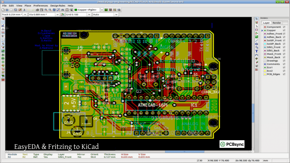
Working with BRD Files in KiCad
The .brd extension gets confusing because both older KiCad versions and Eagle used it. Here’s how to handle different scenarios:
Eagle .brd Files
Import through File → Import → Non-KiCad Board File and select “Autodesk Eagle Board Files” from the file type dropdown.
Legacy KiCad .brd Files
If you have old KiCad projects (pre-version 4) with .brd extensions, modern KiCad opens these automatically. The file will be converted to .kicad_pcb format when you save.
Identifying the Source
Not sure what created a .brd file? Open it in a text editor. Eagle .brd files are XML (version 6+) or binary (older versions). Old KiCad .brd files start with “PCBNEW-BOARD Version”.
Converting from KiCad to Altium or Eagle
Sometimes you need to go the other direction—sending files to a client who uses Altium or collaborating with a team stuck on Eagle.
KiCad to Altium
Altium Designer includes a native KiCad import wizard:
In Altium, go to File → Import Wizard
Select “KiCad Design Files” (may require enabling the extension under Extensions & Updates)
Add your .kicad_sch and .kicad_pcb files
Map symbols and footprints as prompted
Configure output directories and click Finish
The import quality varies—complex designs may require cleanup, and custom footprints sometimes need adjustment.
KiCad to Eagle
Unfortunately, Eagle never implemented KiCad import functionality. Autodesk’s support team has acknowledged requests for this feature but hasn’t delivered it. Your options are limited to:
Exporting Gerbers from KiCad and importing those into Eagle (layout only, no editability)
Manual recreation of the design
Third-party conversion services (use with caution)
Allegro to KiCad Conversion
Cadence Allegro uses proprietary binary formats that KiCad doesn’t natively support. However, there are workarounds:
Using the System76 Converter
System76 developed a Rust-based Allegro to KiCad converter for their internal use and released it as open source:
This handles Allegro extract files but may not support all features.
IDF Export/Import
For board outline and component placement, you can export from Allegro as IDF (Intermediate Data Format) and import into KiCad. This won’t bring in traces or routing but gives you a starting point.
Common Conversion Issues and Solutions
Missing Footprints After Import
Problem: Components appear in the schematic but lack footprint assignments in the PCB.
Solution: Open Symbol Editor, locate the affected symbols, and manually assign footprints using the footprint field. Run “Update PCB from Schematic” to sync.
Broken Net Connections
Problem: The DRC shows unconnected items that were connected in the original design.
Solution: This often happens with power symbols and global labels. Check that net names match exactly, including case sensitivity. KiCad treats “VCC” and “Vcc” as different nets.
Layer Misalignment
Problem: Copper pours or tracks appear on wrong layers.
Solution: Review your layer mapping and re-import if necessary. For minor issues, select affected objects and use Edit → Change Layer.
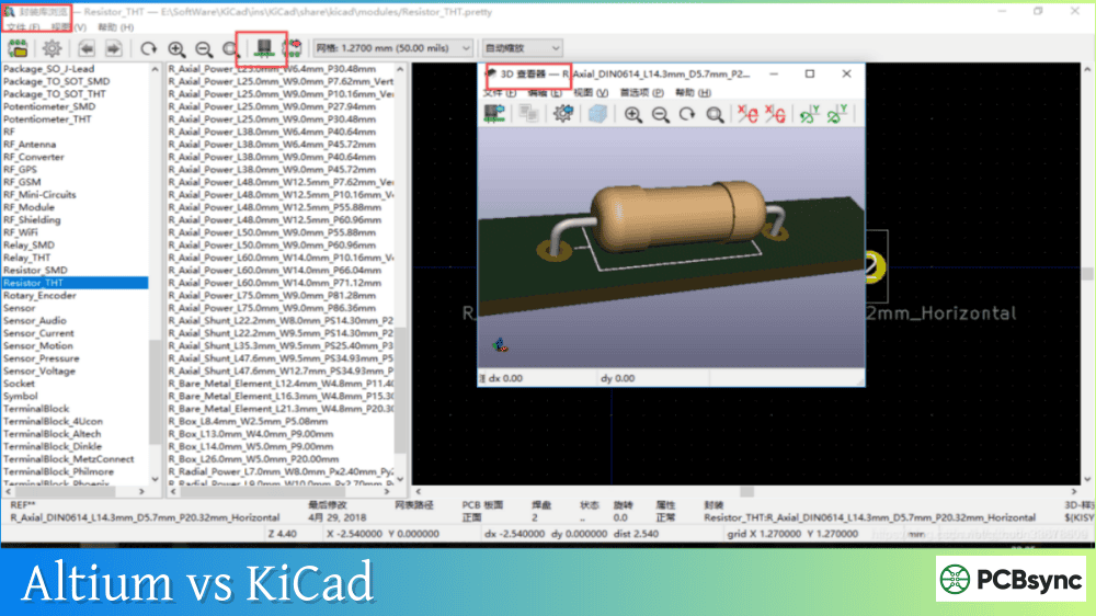
3D Model Conversion
Problem: STEP files from Altium don’t appear in KiCad’s 3D viewer.
Solution: KiCad prefers WRL (VRML) format for 3D models. Use FreeCAD to batch-convert STEP files:
Open FreeCAD and load the STEP file
Export as VRML (.wrl)
Update the footprint’s 3D model path in KiCad
Best Practices for Successful Migration
Based on my experience with hundreds of conversions, here’s what works:
Always convert a test project first. Don’t migrate your most complex board on day one. Start with something simple to understand the quirks.
Keep original files intact. Conversion is one-way. Store your Altium or Eagle files somewhere safe before starting.
Document your layer mapping. If you establish a consistent mapping scheme, create a reference document for future projects.
Verify against Gerbers. Generate Gerber files from both the original and converted designs, then overlay them in a Gerber viewer to spot discrepancies.
Update libraries post-migration. Don’t just use imported libraries indefinitely. Gradually replace them with native KiCad symbols and footprints to avoid compatibility issues in future KiCad versions.
Can I convert Altium projects to KiCad without owning Altium?
Yes. KiCad’s native importer reads Altium files directly without needing Altium installed. The altium2kicad converter also works independently. You only need access to the source files (.SchDoc, .PcbDoc, etc.).
Will my design rules transfer during conversion?
Generally, no. Design rules (trace width, clearance, via sizes) rarely survive conversion intact between any EDA tools. Plan to manually recreate your DRC rules in KiCad after importing the layout. This is actually a good opportunity to review and update your design rules.
How do I handle multi-sheet schematics from Eagle or Altium?
KiCad supports hierarchical schematics. When importing, select the top-level schematic file, and KiCad will attempt to pull in referenced sub-sheets. For flat multi-sheet designs, you may need to import each sheet separately and then establish the hierarchy in KiCad.
My converted PCB shows DRC errors everywhere. Is this normal?
Some DRC errors after import are expected. Missing net connections, clearance violations, and unconnected pins often result from format differences. The key is distinguishing between false positives from import artifacts versus genuine design issues. Review each error type systematically.
Is there a way to automate batch conversion of multiple projects?
For Eagle projects, the ULP scripts can be modified for batch processing. For Altium, you’d need to script around the command-line import options or use the altium2kicad Perl converter with shell scripting. The KiCad community forum has several threads with batch conversion solutions that others have shared.
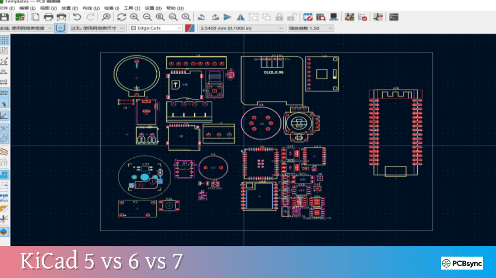
Version Compatibility Matrix
Understanding which KiCad version you need matters for successful conversion. Here’s what each major release supports:
Feature
KiCad 6
KiCad 7
KiCad 8
KiCad 9
Eagle Project Import
Yes
Yes
Yes
Yes
Altium Schematic (.SchDoc)
No
Yes
Yes
Yes
Altium PCB (.PcbDoc)
No
Yes
Yes
Yes
Altium Symbol Library (.SchLib)
No
No
Yes
Yes
Altium Footprint Library (.PcbLib)
No
Partial
Yes
Yes
Altium Integrated Library (.IntLib)
No
No
Yes
Yes
Altium Project File (.PrjPcb)
No
No
No
Yes (9.0.3+)
Eagle Library Import (.lbr)
Via script
Via script
Direct
Direct
For the smoothest experience, use KiCad 9 or later. The import capabilities improve significantly with each release, and bug fixes address many edge cases that caused problems in earlier versions.
Real-World Migration Scenarios
Let me share some actual situations I’ve encountered and how to handle them:
Scenario 1: Inheriting a TI Reference Design
Texas Instruments publishes reference designs in Altium format. To use these in KiCad:
Download the .zip file from TI’s website
Extract and locate the .SchDoc and .PcbDoc files
Import the PCB first using KiCad’s native importer
Import each schematic sheet
Expect to spend time fixing net names—TI uses specific naming conventions
Replace TI’s proprietary footprints with standard ones where possible
Scenario 2: Migrating a Company Library
Moving years of accumulated Eagle libraries requires a systematic approach:
Audit your existing library—identify what you actually use versus legacy parts
Convert high-priority components first using eagle-lbr2kicad
Validate each footprint against datasheets (conversion errors happen)
Build a verification checklist covering pad sizes, pin numbering, and 3D models
Create a library style guide for your team to maintain consistency
Scenario 3: Collaborating with External Teams
When you use KiCad but your manufacturing partner expects Altium files:
Export Gerbers and drill files—these are universal
Provide ODB++ or IPC-2581 format if they need intelligent data
For schematic review, export PDFs with the built-in BOM
Consider using Altium 365 Viewer links for interactive collaboration
Troubleshooting Guide for Specific Errors
“Failed to parse” Errors
This typically means the source file is corrupted or uses features the importer doesn’t recognize. Try opening the file in its native application first, saving a fresh copy, and then importing that copy.
Components Scattered Off-Board
After import, footprints sometimes appear at coordinates far from the board outline. This happens when the original design used a different coordinate origin. In KiCad’s PCB Editor, select all components (Ctrl+A) and use Edit → Move Exactly to relocate them to sensible positions.
Net Names with Special Characters
Altium allows characters in net names that KiCad doesn’t handle well. During import, these get mangled or cause connection errors. You may need to rename nets in the original design before converting, or manually fix net names in KiCad after import.
Polygon Pours Not Filling
If copper pours appear empty after import, the zone priority or clearance settings may be wrong. Select the zone, open its properties, and verify the net assignment. Then click “Edit Zone → Fill Zone” or press B to refill all zones.
Post-Conversion Checklist
Use this checklist after every conversion to ensure nothing was lost:
Schematic Verification:
All components present with correct values
All net connections intact
Power symbols properly connected
Hierarchical sheet references working
No ERC errors (or only expected ones)
PCB Verification:
Board outline matches original dimensions
All layers present and correctly mapped
Component count matches schematic
No orphaned vias or traces
Copper pours properly filled
Drill files generate correctly
Library Verification:
Footprint pad sizes match datasheets
Pin numbering correct
Courtyard and silkscreen appropriate
3D models assigned where needed
Wrapping Up
Converting Altium to KiCad or Eagle to KiCad isn’t just about file formats—it’s about preserving your engineering work while moving to a tool that gives you more control. The process has gotten dramatically easier with recent KiCad releases, and the community continues to improve import capabilities.
My recommendation: if you’re planning a migration, start now while both your old and new tools are available. Convert a few test projects, establish your workflow, and document your layer mappings. The time investment pays off when you eventually need to migrate production designs or collaborate with teams using different tools.
The open-source nature of KiCad means you’re never locked in again. Your designs remain yours, in formats you can read and manipulate without expensive subscriptions or license servers. That freedom is worth the effort of conversion.
Whether you’re moving from EagleCad to KiCad because of Autodesk’s discontinuation, switching from Altium Designer to KiCad to reduce licensing costs, or exploring Allegro to KiCad conversion for specific projects, the path forward is clearer than ever. Start with the native importers, fall back to third-party tools when needed, and always verify your results against the original design.
Inquire: Call 0086-755-23203480, or reach out via the form below/your sales contact to discuss our design, manufacturing, and assembly capabilities.
Quote: Email your PCB files to Sales@pcbsync.com (Preferred for large files) or submit online. We will contact you promptly. Please ensure your email is correct.
Notes: For PCB fabrication, we require PCB design file in Gerber RS-274X format (most preferred), *.PCB/DDB (Protel, inform your program version) format or *.BRD (Eagle) format. For PCB assembly, we require PCB design file in above mentioned format, drilling file and BOM. Click to download BOM template To avoid file missing, please include all files into one folder and compress it into .zip or .rar format.


