Inquire: Call 0086-755-23203480, or reach out via the form below/your sales contact to discuss our design, manufacturing, and assembly capabilities.
Quote: Email your PCB files to Sales@pcbsync.com (Preferred for large files) or submit online. We will contact you promptly. Please ensure your email is correct.
Notes: For PCB fabrication, we require PCB design file in Gerber RS-274X format (most preferred), *.PCB/DDB (Protel, inform your program version) format or *.BRD (Eagle) format. For PCB assembly, we require PCB design file in above mentioned format, drilling file and BOM. Click to download BOM template To avoid file missing, please include all files into one folder and compress it into .zip or .rar format.
Altium Designer Tutorial for Beginners: Learn PCB Design Step-by-Step
Learning PCB design can feel overwhelming when you’re staring at a blank schematic for the first time. Trust me, I remember that feeling well. But here’s the good news: Altium Designer makes the process far more intuitive than you might expect, and this Altium Designer tutorial for beginners will walk you through every essential step.
Whether you’re a student tackling your first electronics project, a hobbyist ready to move beyond breadboards, or an engineer transitioning from another EDA tool, this guide covers the complete workflow from project creation through manufacturing output. By the end, you’ll have the confidence to design your own PCBs in Altium Designer.
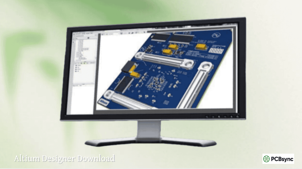
Before diving into design, you need the software up and running. Here’s how to get started:
Visit the Altium website and create a free account
Download the Altium Designer installer from the download page
Run the installer and follow the setup wizard
Launch Altium Designer and sign in with your Altium account
Activate your license through the License Management view
Altium offers a 30-day trial for new users, which gives you full access to evaluate the software. Students can often access extended trials or educational licenses through their institutions.
Understanding the Altium Designer Interface
When you first open Altium Designer, the interface can seem complex. Let’s break down the key elements:
Main Menu Bar: Located at the top, this provides access to all commands organized by category (File, Edit, View, Project, etc.).
Ribbon Interface: Below the menu bar, context-sensitive ribbons display tools relevant to your current activity. The ribbon changes based on whether you’re editing a schematic, PCB, or library.
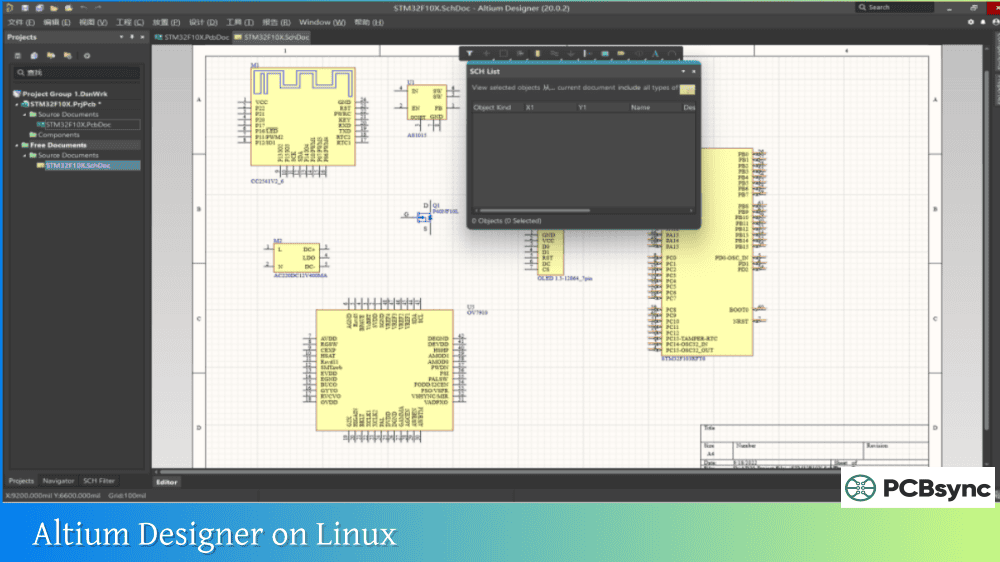
Projects Panel: Typically docked on the left, this panel shows your project structure including all associated files.
Properties Panel: Displays and allows editing of properties for selected objects.
Design Space: The central area where you create your schematic and PCB designs.
Active Bar: A floating toolbar providing quick access to commonly used placement commands.
Creating Your First PCB Project
Every design in Altium Designer begins with a project. The project file (.PrjPcb) ties together all your design documents—schematics, PCB layout, libraries, and output files.
Setting Up a New Project
Follow these steps to create your first project:
Select File → New → Project → PCB Project
In the Create Project dialog, enter a name for your project
Choose a location to save your project files
Click Create to generate the project
Your new project appears in the Projects panel, initially showing “No Documents Added.” We’ll add documents as we progress through the design.
Adding Design Documents
A typical PCB project requires at least two documents:
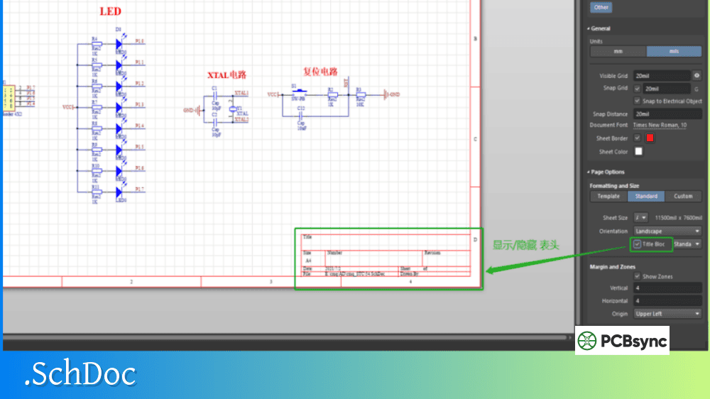
Schematic Document (.SchDoc): Contains your circuit design with component symbols and electrical connections.
PCB Document (.PcbDoc): Contains the physical board layout with component footprints and copper traces.
To add a schematic:
Right-click your project in the Projects panel
Select Add New to Project → Schematic
Save the schematic with a meaningful name (File → Save As)
To add a PCB document:
Right-click your project in the Projects panel
Select Add New to Project → PCB
Save the PCB with a matching name
Schematic Design Basics
The schematic captures your circuit’s electrical design. This is where you define what components you need and how they connect together.
Placing Components on Your Schematic
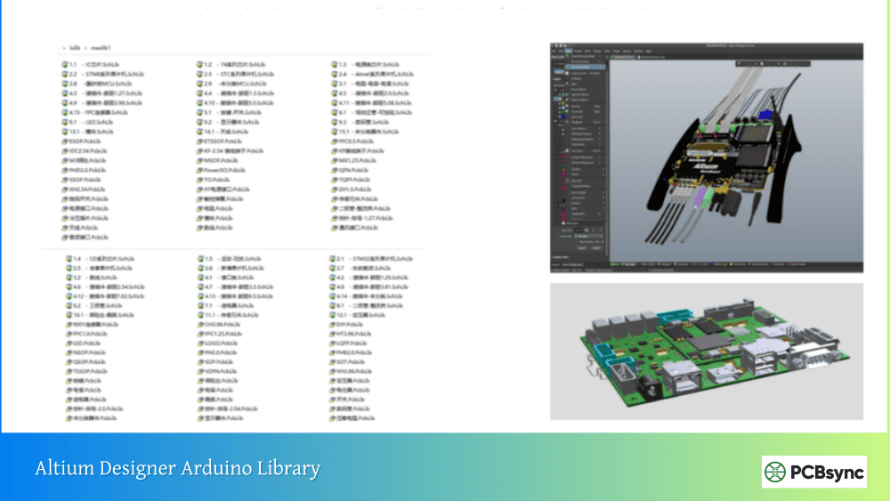
Components come from libraries. Altium provides extensive built-in libraries, and you can access millions more through the Manufacturer Part Search or Altium 365.
To place a component:
Press P, P (Place Part) or use the Components panel
Search for your component by part number or description
Click to place the component on your schematic
Press Spacebar to rotate the component before placing
Press X or Y to flip the component horizontally or vertically
Click to confirm placement, or right-click to exit placement mode
When placing multiple identical components, keep clicking to place additional instances. The designator automatically increments (R1, R2, R3, etc.).
Wiring Your Circuit
Once components are placed, you need to connect them electrically:
Press P, W to start placing wires
Click on a component pin to start the wire
Click to add corners as needed
Click on the destination pin to complete the connection
Right-click or press Escape to exit wire mode
Pro tip: Use net labels for connections that would require long, crossing wires. Press P, N to place a net label. Components sharing the same net label name are electrically connected without visible wires.
Annotating Your Schematic
Before transferring your design to PCB, every component needs a unique designator. While you can manually assign these, Altium’s annotation tool handles this automatically:
Select Tools → Annotation → Annotate Schematics
Choose your preferred annotation order (typically “Up Then Across” or “Down Then Across”)
Click Update Changes List to preview assignments
Click Accept Changes to apply the annotations
Click Execute Changes to finalize
Running Electrical Rule Checks
Before proceeding to layout, verify your schematic has no electrical errors:
Select Project → Compile PCB Project
Review any warnings or errors in the Messages panel
Double-click an error to jump directly to the problem location
Fix issues and recompile until the design is error-free
Common errors include unconnected pins, duplicate designators, and missing power connections.
Transferring Your Design to PCB
With a complete, error-free schematic, you’re ready to create the physical board layout.
Synchronizing Schematic to PCB
Altium uses an Engineering Change Order (ECO) process to transfer design data:
The Engineering Change Order dialog appears showing proposed changes
Click Validate Changes to check for problems
Click Execute Changes to transfer the design
Click Close when complete
Your component footprints now appear in the PCB editor, clustered together outside the board outline. Connection lines (ratsnest) show the required connections between pads.
Setting Up Your PCB
Before placing components, configure your board:
Define the Board Shape:
Switch to the PCB editor
Select Design → Edit Board Shape
Click to define corners of your board outline
Press Escape to close the shape
Set Up the Layer Stack:
Select Design → Layer Stack Manager
For a simple two-layer board, the default stack works fine
For more complex designs, add layers as needed
Save changes with File → Save to PCB
Configure Design Rules:
Select Design → Rules
Set clearance rules based on your manufacturer’s capabilities
Configure routing width rules for signal and power traces
Define via sizes appropriate for your fabricator
Rule Type
Typical Value
Purpose
Clearance
0.15-0.2mm
Minimum space between copper objects
Track Width
0.2-0.3mm
Default routing width
Via Diameter
0.6mm
Outer diameter of vias
Via Hole
0.3mm
Drill hole size for vias
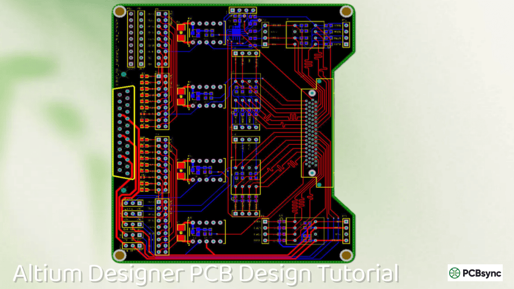
PCB Layout and Component Placement
Good component placement is crucial. As experienced designers say, PCB design is 90% placement and 10% routing.
Component Placement Guidelines
Follow these principles for effective placement:
Start with fixed-position components: Connectors, mounting holes, and components with mechanical constraints go first.
Place major components next: Microcontrollers, processors, and other central ICs define your layout’s overall organization.
Group related components: Keep bypass capacitors near their associated ICs. Place components that connect together close to each other.
Consider signal flow: Arrange components so signals flow logically across the board, typically left-to-right or input-to-output.
Leave routing space: Don’t pack components so tightly that routing becomes impossible.
Moving and Rotating Components
Basic placement controls:
Click and drag to move components
Spacebar rotates by 90° while dragging
L key flips a component to the opposite layer while dragging
M, M (Move, Move) selects a component under the cursor for moving
To move components precisely:
Select the component
Press M then M for Move command
Click the component’s reference point
Type coordinates or click the destination
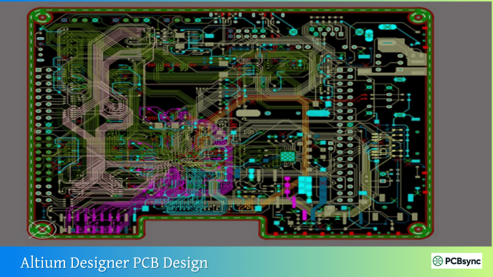
Routing Your PCB
Routing connects component pads with copper traces, transforming connection lines into actual electrical paths.
Interactive Routing Basics
To start routing:
Press P, T (Place Track) or click the Interactive Routing button
Click on a pad to start the route
Move the cursor toward the destination
Click to place corners
Click on the destination pad to complete the route
Press Escape to cancel the current route
Essential routing shortcuts:
Shortcut
Action
Tab
Open routing properties (width, via style)
Shift+Spacebar
Cycle through corner modes (45°, 90°, arc)
Shift+W
Select from predefined track widths
* (asterisk)
Switch between routing layers
+ / –
Step through enabled layers
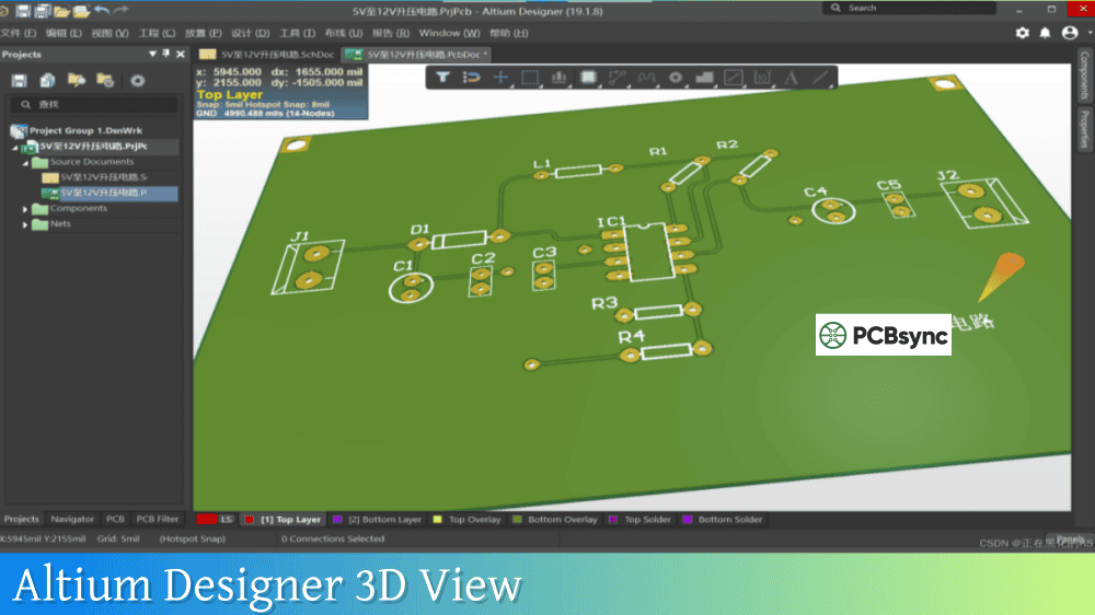
3
Switch to 3D view
2
Return to 2D view
Routing Tips for Beginners
Route critical signals first: Power, ground, and high-speed signals deserve priority and the most direct paths.
Avoid 90° corners: Use 45° angles or curved corners for better signal integrity and manufacturability.
Maintain adequate spacing: Don’t run traces closer together than necessary. Extra spacing reduces crosstalk.
Use ground planes: For two-layer boards, consider using the bottom layer primarily as a ground plane with signal routing on top.
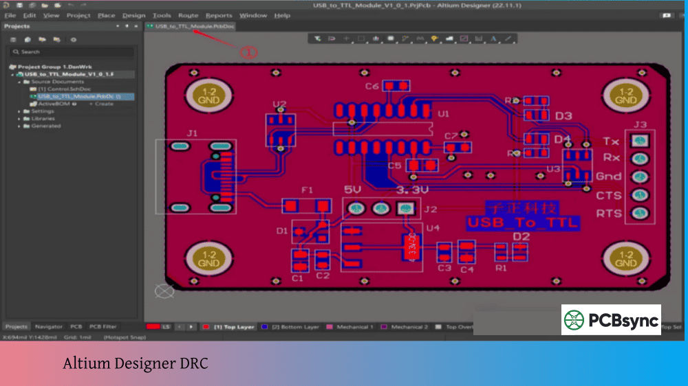
Check as you go: Run Design Rule Check (DRC) periodically to catch errors early. Press T, D, R to run DRC.
Placing Vias
When you need to switch layers during routing:
While routing, press ***** (asterisk) or +/- to change layers
A via is automatically inserted at the layer transition
Continue routing on the new layer
You can also place vias manually with P, V (Place Via).
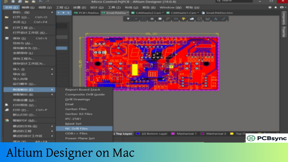
3D PDFs: 3D representations for assembly verification
Essential Keyboard Shortcuts Reference
Mastering shortcuts dramatically improves your productivity. Here are the most important ones:
Category
Shortcut
Action
General
Ctrl+S
Save
Ctrl+Z
Undo
Ctrl+M
Measure distance
Q
Toggle metric/imperial units
V, F
Fit view to show all objects
Schematic
P, P
Place part
P, W
Place wire
P, N
Place net label
T, A, A
Open annotation dialog
PCB
P, T
Interactive routing
P, V
Place via
P, G
Place polygon pour
L
Show layer visibility dialog
Shift+S
Toggle single layer mode
2
2D view
3
3D view
Routing
Tab
Routing properties
Shift+Space
Cycle corner modes
*
Switch routing layer
Useful Resources for Learning Altium Designer
Official Altium Resources
Resource
Description
Altium Designer Documentation
Comprehensive official documentation
Altium Academy
Video tutorials and courses
Altium 365 Viewer
Free online viewer for Altium projects
Altium Designer Trial
30-day free trial download
Community Resources
Resource
Description
Altium Designer Forum
Official community forums
Phil’s Lab (YouTube)
Excellent PCB design tutorials
Robert Feranec (YouTube)
Professional PCB design content
EEVblog Forum
Active electronics community
Component Resources
Resource
Description
Octopart
Component search with CAD models
SnapEDA
Free schematic symbols and footprints
Ultra Librarian
CAD model downloads
Manufacturer Part Search
Built-in Altium component search
Frequently Asked Questions
How long does it take to learn Altium Designer?
Most engineers can complete a basic two-layer design within a few days of focused learning. Becoming proficient with advanced features like high-speed design, rigid-flex, and scripting takes months of practice. The good news is that Altium’s consistent interface means skills you learn early apply throughout the software.
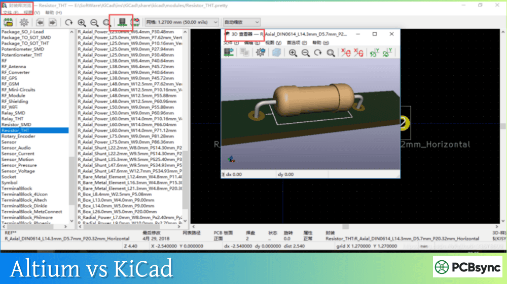
Can I open EAGLE or KiCad files in Altium Designer?
Yes, Altium Designer can import designs from several other EDA tools including EAGLE, KiCad, OrCAD, and PADS. Select File → Import Wizard and choose the appropriate source format. While import quality varies depending on design complexity, most designs transfer successfully with minor cleanup needed.
What’s the difference between schematic symbols and PCB footprints?
Schematic symbols represent the electrical function of a component—they show pins and their relationships but have no physical dimensions. PCB footprints represent the physical pads and outlines that exist on the manufactured board. Every component needs both a symbol (for the schematic) and a footprint (for the PCB) linked together.
Do I need an internet connection to use Altium Designer?
Altium Designer can work offline once installed and licensed, though some features benefit from connectivity. The Manufacturer Part Search, Altium 365 collaboration, and some library features require internet access. You can design complete boards offline, but periodic connection helps keep libraries and the software updated.
How do I choose the right number of layers for my design?
Start simple. Most hobby projects and many professional designs work fine with two layers. Consider four layers when you have significant power distribution requirements, many components, or high-speed signals needing controlled impedance. More layers add cost and complexity, so don’t overengineer. If you’re unsure, try routing with two layers first—you can always add more if needed.
Next Steps in Your PCB Design Journey
Completing this Altium Designer tutorial for beginners gives you the foundation to create real PCB designs. But learning doesn’t stop here. As you gain experience, explore these advanced topics:
Component Library Creation: Building your own component libraries ensures accuracy and speeds future designs.
Design for Manufacturing (DFM): Understanding manufacturer capabilities helps you design boards that fabricate reliably.
High-Speed Design: Learn about controlled impedance, differential pairs, and signal integrity for faster designs.
Multi-Layer Stackups: Master complex layer configurations for dense, high-performance boards.
Altium 365: Explore cloud collaboration features for team-based design projects.
The best way to improve is through practice. Pick a project—maybe recreating an existing circuit or designing something new—and work through the complete process. Each design teaches lessons that make the next one easier.
Welcome to the world of PCB design. Your first manufactured board, when it arrives and works, delivers a satisfaction that makes all the learning worthwhile.
Inquire: Call 0086-755-23203480, or reach out via the form below/your sales contact to discuss our design, manufacturing, and assembly capabilities.
Quote: Email your PCB files to Sales@pcbsync.com (Preferred for large files) or submit online. We will contact you promptly. Please ensure your email is correct.
Notes: For PCB fabrication, we require PCB design file in Gerber RS-274X format (most preferred), *.PCB/DDB (Protel, inform your program version) format or *.BRD (Eagle) format. For PCB assembly, we require PCB design file in above mentioned format, drilling file and BOM. Click to download BOM template To avoid file missing, please include all files into one folder and compress it into .zip or .rar format.


