Inquire: Call 0086-755-23203480, or reach out via the form below/your sales contact to discuss our design, manufacturing, and assembly capabilities.
Quote: Email your PCB files to Sales@pcbsync.com (Preferred for large files) or submit online. We will contact you promptly. Please ensure your email is correct.
Notes: For PCB fabrication, we require PCB design file in Gerber RS-274X format (most preferred), *.PCB/DDB (Protel, inform your program version) format or *.BRD (Eagle) format. For PCB assembly, we require PCB design file in above mentioned format, drilling file and BOM. Click to download BOM template To avoid file missing, please include all files into one folder and compress it into .zip or .rar format.
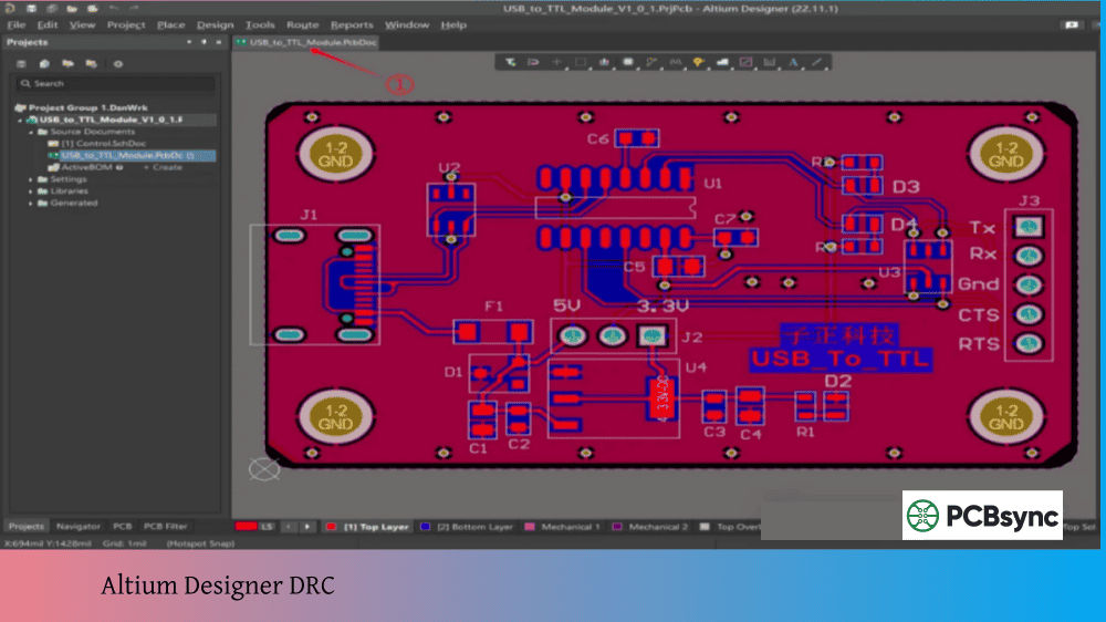
Altium Designer DRC: How to Set Up Design Rule Checks
Nothing ruins your week quite like getting boards back from fabrication only to discover that two traces are shorted because they were 0.5 mils too close together. Or realizing your vias are too small for the manufacturer’s capabilities. Or finding that a component footprint overlaps another by a fraction of a millimeter. These are exactly the kinds of problems that Altium Designer DRC exists to prevent.
Design Rule Checking is the safety net that catches manufacturing issues before they become expensive mistakes. I’ve been using Altium for over a decade, and I can confidently say that a well-configured DRC has saved me from costly respins more times than I can count. This guide walks you through setting up design rules properly, running checks effectively, and resolving violations efficiently.
Before diving into configuration, it helps to understand what the DRC system actually does and how it operates.
What Design Rule Checking Does
DRC is an automated verification system that checks your PCB layout against a defined set of rules. These rules represent the physical and electrical constraints of your design—things like minimum trace widths, clearances between objects, via sizes, and manufacturing limits. When any object in your design violates a rule, Altium flags it as a violation.
Think of design rules as an instruction set for the PCB editor. They tell Altium what’s acceptable and what isn’t, allowing the software to monitor your work and alert you when something goes wrong.
Online DRC vs Batch DRC
Altium provides two modes of design rule checking:
Mode
Description
When to Use
Online DRC
Checks rules in real-time as you work
During active design and routing
Batch DRC
Runs a complete check on demand
Before sending to fabrication, after major changes
Online DRC monitors your design continuously. When you place a trace too close to a pad, the violation appears immediately. This real-time feedback prevents you from building up hundreds of violations that become overwhelming to fix later.
Batch DRC performs a comprehensive check of all enabled rules at once. It’s more thorough than Online DRC because it can check rules that would be too computationally expensive to run continuously. Always run a Batch DRC before generating manufacturing outputs.
Important: Online DRC only detects new violations created after it’s enabled. It won’t catch existing violations. That’s why starting and ending every design with a Batch DRC is essential.
Accessing the PCB Rules and Constraints Editor
Design rules are configured in the PCB Rules and Constraints Editor. There are two ways to access it, depending on your project setup.
Method 1: PCB Rules and Constraints Editor (Traditional)
Open your PCB document
Go to Design → Rules (or press D, R)
The PCB Rules and Constraints Editor dialog opens
This is the traditional approach and works for all Altium Designer versions.
Method 2: Constraint Manager (Newer Projects)
If your project was created with Constraint Management enabled:
Open your schematic or PCB document
Go to Design → Constraint Manager
Configure constraints in the matrix-based interface
The Constraint Manager provides a more visual approach to defining clearances and widths, particularly useful for complex designs with multiple net classes.
Note: If you don’t see the Rules command in the Design menu, your project is using the Constraint Manager instead. The two systems are mutually exclusive—you use one or the other, not both.
Essential Design Rule Categories
Altium organizes design rules into categories. Understanding these categories helps you configure the right rules for your design.
Design Rule Categories Overview
Category
Purpose
Key Rules
Electrical
Prevents shorts and ensures connectivity
Clearance, Short-Circuit, Un-Routed Net
Routing
Controls trace characteristics
Width, Routing Layers, Via Style, Differential Pairs
For most designs, you’ll spend the majority of your time configuring Electrical, Routing, and Manufacturing rules.
Setting Up Clearance Rules
Clearance rules define the minimum distance between electrical objects. They’re the most critical rules for preventing shorts and ensuring manufacturability.
Configuring Basic Clearance
In the PCB Rules and Constraints Editor, expand Electrical → Clearance
Select the default Clearance rule
Set your minimum clearance value
The clearance constraint uses a matrix that lets you define different clearances between different object types:
Object Type
Common Clearance Setting
Track to Track
6-8 mils (0.15-0.2mm)
Track to Pad
6-8 mils
Track to Via
6-8 mils
Pad to Pad
6-8 mils
Via to Via
6-8 mils
Track to Polygon
10-12 mils
Hole to Hole
10-15 mils
Pro tip: Check with your PCB manufacturer for their minimum capabilities. Many low-cost fabricators can achieve 6 mil clearance reliably, but going smaller increases cost.
Creating Net Class-Specific Clearance Rules
High-voltage nets or sensitive analog signals often need larger clearances. Create additional rules for these:
Right-click on Clearance and select New Rule
Name the rule descriptively (e.g., “HighVoltage_Clearance”)
Set the scope using a query like InNetClass(‘HighVoltage’)
Set the higher clearance value
Ensure priority is higher (lower number) than the default rule
Configuring Routing Width Rules
Width rules control trace thickness, which affects current carrying capacity, impedance, and manufacturability.
Setting Up Basic Width Rules
Expand Routing → Width
Select the default Width rule
Configure three values:
Minimum Width: Absolute minimum allowed
Preferred Width: What the router targets
Maximum Width: Upper limit
Recommended Width Settings
Net Type
Min Width
Preferred Width
Max Width
Signal traces
4-6 mils
6-8 mils
20 mils
Power traces
10 mils
20-40 mils
100 mils
High-current
20 mils
50-100 mils
200 mils
Creating Power Net Width Rules
Power and ground traces typically need to be wider than signal traces:
Create a new Width rule
Set scope to InNetClass(‘Power’) or Net = ‘VCC’ OR Net = ‘GND’
Set wider width values
Assign higher priority than the default rule
Setting Up Via Rules
Via rules control the size and style of vias used during routing.
Configuring Routing Via Style
Expand Routing → Routing Via Style
Select or create a rule
Set via parameters:
Parameter
Description
Typical Value
Via Diameter
Outer pad size
20-30 mils
Via Hole Size
Drill diameter
10-15 mils
Via Solder Mask Expansion
Mask opening
2-4 mils or tented
Manufacturing consideration: Smaller vias cost more. Standard via capabilities at most fabs are around 10 mil hole / 20 mil pad. Going smaller often adds cost.
Configuring Manufacturing Rules
Manufacturing rules ensure your design is fabricable. These catch issues that might not cause electrical problems but will fail during production.
Minimum Annular Ring
The annular ring is the copper ring around a drilled hole. If it’s too small, the drill might break through the pad.
Expand Manufacturing → Minimum Annular Ring
Set the minimum value (typically 5-8 mils)
Hole Size Rules
Expand Manufacturing → Hole Size
Set minimum and maximum hole sizes based on manufacturer capabilities
Board Outline Clearance
Objects placed too close to the board edge can be damaged during routing or depanelization.
Expand Manufacturing → Board Outline Clearance
Set clearance values (typically 10-20 mils minimum)
Configure the matrix for different object types if needed
Silk to Solder Mask Clearance
Silkscreen printing over exposed copper pads causes soldering problems.
Expand Manufacturing → Silk To Solder Mask Clearance
Enable “Check Clearance to Solder Mask Openings”
Set appropriate clearance (0-2 mils typically)
Running a Batch Design Rule Check
After configuring your rules, run a comprehensive check before generating outputs.
How to Run Batch DRC
Go to Tools → Design Rule Check (or press T, D)
The Design Rule Checker dialog opens
In the left pane, expand Rules To Check
Enable/disable rules for Batch checking as needed
Click on Report Options to configure output
Enable Create Report File if you want documentation
Click Run Design Rule Check
Understanding the DRC Report
After running the check, violations appear in the Messages panel. The report shows:
Each rule that was tested
Pass/fail status for each rule
Detailed list of violations with locations
Total violation count
A clean DRC report with zero violations is your goal before manufacturing.
Resolving DRC Violations
When violations occur, Altium provides several tools to find and fix them.
Using the PCB Rules and Violations Panel
Open via View → Panels → PCB Rules And Violations
The panel shows all rule classes with violation counts
Click a rule class to see specific violations
Click a violation to zoom to its location in the design
Three Ways to Resolve Violations
Approach
When to Use
How
Fix the violation
Most common
Move, resize, or reroute the offending object
Modify the rule
When rule is too strict
Adjust the rule constraint to match design intent
Waive the violation
Intentional violations
Mark as acceptable without changing rule or object
Waiving Intentional Violations
Sometimes violations are intentional—like a connector hanging over the board edge. Rather than creating complex rules, waive the violation:
Select the violation in the PCB Rules And Violations panel
Right-click and choose Waive Selected Violations
Enter a reason in the Waived Violation Info dialog
The violation moves to the Waived Violations section
Waived violations remain documented and can be unwaived later if needed.
Altium Default Rules: Included with new PCB documents
Frequently Asked Questions About Altium Designer DRC
Why does Online DRC miss some violations that Batch DRC catches?
Online DRC is optimized for real-time performance, so it only checks a subset of rules and only detects new violations created after it’s enabled. Batch DRC performs a comprehensive check of all enabled rules against the entire design. Some rules, like complex polygon checks or certain manufacturing rules, are too computationally expensive for continuous monitoring. Always run a Batch DRC before manufacturing—never rely solely on Online DRC.
How do I fix clearance violations between pads I can’t move?
When component pads violate clearance rules but you can’t change the footprint, you have several options. First, verify the footprint is correct—sometimes library errors cause the issue. If the footprint is correct, check if your manufacturer can actually handle the clearance. If so, either modify the clearance rule to allow that specific situation using a targeted query scope, or waive the violation with documentation explaining why it’s acceptable.
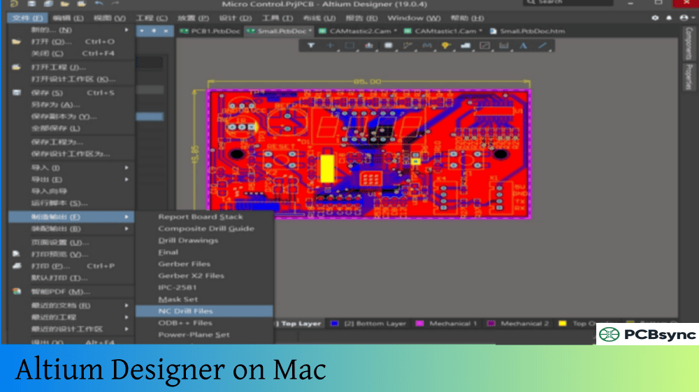
Can I import design rules from my PCB manufacturer?
Yes, many manufacturers provide downloadable rule files (.RUL format) configured for their capabilities. To import: go to Design → Rules, right-click in the rules tree, and select Import Rules. Browse to the .RUL file and import. Review the imported rules and adjust priorities as needed. JLCPCB, for example, provides rule files for their standard capabilities that you can download from their help center.
What’s the difference between the PCB Rules Editor and Constraint Manager?
The PCB Rules and Constraints Editor is the traditional, dialog-based interface for configuring design rules. The Constraint Manager is a newer, matrix-based approach that’s enabled when creating a project. The main difference is workflow—Constraint Manager is more visual for clearance and width settings and allows defining constraints from the schematic side. You use one or the other, not both. If you don’t see Design → Rules, your project uses Constraint Manager; access it via Design → Constraint Manager instead.
How do I handle DRC violations for deliberately placed objects like board edge connectors?
For intentional violations like connectors extending beyond the board edge, use Altium’s waive feature rather than disabling the rule entirely. Select the violations in the PCB Rules And Violations panel, right-click, choose Waive Selected Violations, and document why it’s acceptable. This keeps the rule active for catching real problems while acknowledging that specific violations are intentional. Waived violations are tracked and included in DRC reports with your explanation.
Final Recommendations for Effective DRC
Altium Designer DRC is one of the most valuable tools in your design workflow, but only if you configure and use it properly. Here’s how to get the most from it:
Set up rules before you start designing. Configuring rules after routing means fixing violations you could have prevented. Take the time upfront to match rules to your manufacturer’s capabilities.
Use Online DRC during active design. The real-time feedback prevents violations from accumulating. Yes, it can slow down the editor on complex designs, but the time saved fixing violations more than compensates.
Run Batch DRC at milestones. Don’t wait until the end. Check after placement, after routing sections, and before generating outputs. Early detection means easier fixes.
Document your waivers. When you waive a violation, explain why. Future you (or a colleague) will appreciate knowing that the connector overhang was intentional, not an oversight.
Save your rule sets. Once you have rules configured for a manufacturer, export them. Importing proven rules into new projects saves time and ensures consistency.
A clean DRC report doesn’t guarantee a perfect board, but it dramatically reduces the risk of preventable manufacturing issues. Invest the time in proper DRC configuration—your future self will thank you when boards come back working on the first spin.
Inquire: Call 0086-755-23203480, or reach out via the form below/your sales contact to discuss our design, manufacturing, and assembly capabilities.
Quote: Email your PCB files to Sales@pcbsync.com (Preferred for large files) or submit online. We will contact you promptly. Please ensure your email is correct.
Notes: For PCB fabrication, we require PCB design file in Gerber RS-274X format (most preferred), *.PCB/DDB (Protel, inform your program version) format or *.BRD (Eagle) format. For PCB assembly, we require PCB design file in above mentioned format, drilling file and BOM. Click to download BOM template To avoid file missing, please include all files into one folder and compress it into .zip or .rar format.


