Inquire: Call 0086-755-23203480, or reach out via the form below/your sales contact to discuss our design, manufacturing, and assembly capabilities.
Quote: Email your PCB files to Sales@pcbsync.com (Preferred for large files) or submit online. We will contact you promptly. Please ensure your email is correct.
Notes: For PCB fabrication, we require PCB design file in Gerber RS-274X format (most preferred), *.PCB/DDB (Protel, inform your program version) format or *.BRD (Eagle) format. For PCB assembly, we require PCB design file in above mentioned format, drilling file and BOM. Click to download BOM template To avoid file missing, please include all files into one folder and compress it into .zip or .rar format.
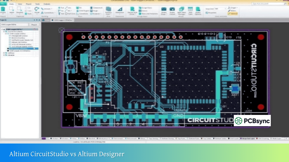
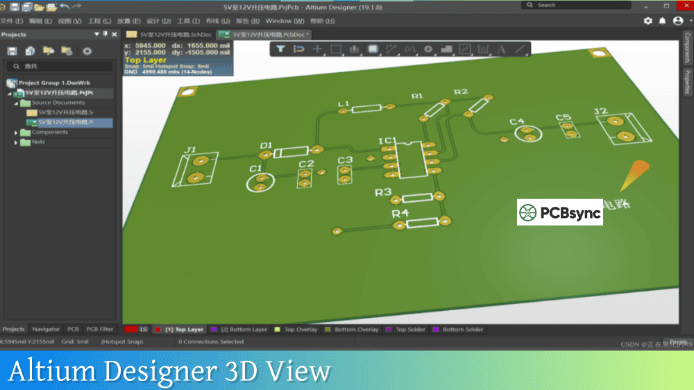
Altium Designer 3D View: How to Visualize Your PCB in 3D
There’s a moment in every PCB project when you realize you need to see your board as more than just layers of colored polygons. Maybe you’re trying to figure out if that tall electrolytic capacitor will fit under the LCD module. Or you need to verify that your connectors line up with the cutouts in the enclosure. Or perhaps you just want to show a client what their finished product will look like. That’s when Altium Designer 3D View becomes indispensable.
I’ve been using Altium’s 3D visualization since the feature was first introduced, and it’s fundamentally changed how I approach PCB design. Being able to see my board as a physical object—complete with components, copper pours, and solder mask—catches problems that would otherwise slip through to fabrication. This guide covers everything you need to know about using 3D visualization effectively in your PCB workflow.
Before diving into the how-to, let’s talk about why you should care about 3D visualization in the first place.
Catching Mechanical Issues Early
The most practical benefit of Altium Designer 3D View is identifying mechanical problems before you commit to fabrication. In 2D, it’s easy to miss that a through-hole component on the bottom of the board collides with a tall IC on the top. In 3D, these conflicts become immediately obvious.
I’ve personally caught dozens of issues using 3D visualization that would have been costly to fix after manufacturing:
Components that wouldn’t fit in the enclosure
Connectors misaligned with panel cutouts
Heat sinks blocking access to adjustment potentiometers
Tall components interfering with mezzanine boards
Silkscreen text hidden under other components
Improved Communication with Stakeholders
Not everyone can read a 2D PCB layout. When you’re presenting to mechanical engineers, clients, or manufacturing partners, a 3D view communicates your design intent far more effectively than colored polygons ever could. You can export high-quality renders or even create flyover videos to demonstrate exactly how the finished board will look.
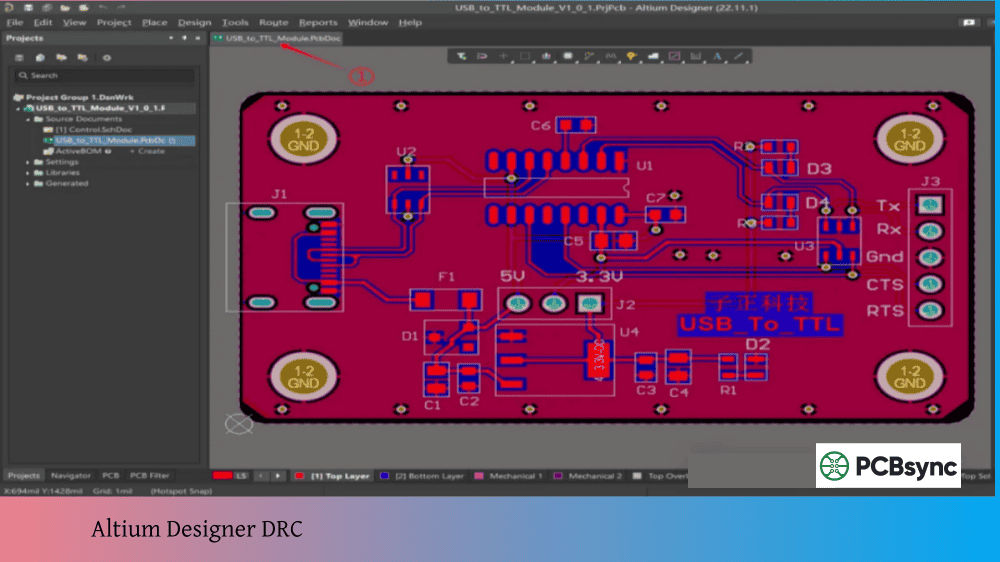
Design Rule Verification in 3D
Altium doesn’t just show you a pretty picture—it actively checks for 3D collisions using the Component Clearance design rules. When two components violate clearance rules in 3D space, the system highlights the violation so you can fix it before generating manufacturing files.
Switching to 3D Layout Mode
Getting into 3D view is straightforward. With your PCB document open:
Quick Access Methods
Method
How to Access
Keyboard shortcut
Press 3
Menu
View → 3D Layout Mode
View Configuration panel
Set 3D option to On in General Settings
To return to 2D view, press 2 or select View → 2D Layout Mode.
Pro tip: When switching between 2D and 3D, Altium remembers your last view in each mode. If you want to maintain your current zoom location when switching, hold Ctrl+Alt while pressing 2 or 3.
Navigating the 3D View
Once you’re in 3D mode, you need to know how to move around. The navigation controls might feel unfamiliar at first, but they become second nature with practice.
Mouse and Keyboard Navigation Controls
Action
Control
Zoom in/out
Ctrl + Mouse wheel or PgUp/PgDn
Pan vertically
Mouse wheel (scroll up/down)
Pan horizontally
Shift + Mouse wheel
Rotate view
Shift + Right-click drag
Flip board
Ctrl + F
Fit board to screen
V, F
Reset rotation
View → Zero Rotation
Using the Navigation Ball
When you hold Shift in 3D mode, a navigation ball (sphere) appears on screen. This provides intuitive control over rotation:
Click and drag on the ball to rotate freely
Click on specific arrows or arcs to rotate around a single axis
The colored arrows correspond to X (red), Y (green), and Z (blue) axes
3D Mouse Support
If you work extensively in 3D, consider investing in a 3D mouse like the 3Dconnexion SpaceMouse. Altium Designer fully supports these devices, allowing you to navigate the 3D view by physically manipulating the controller knob. It’s like holding the actual board in your hand and turning it around to examine different angles.
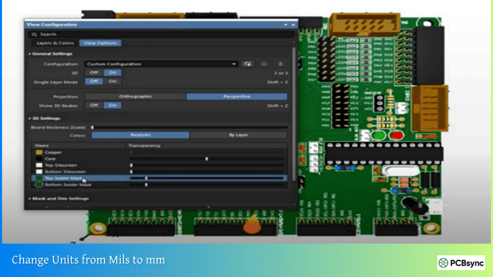
Configuring 3D View Settings
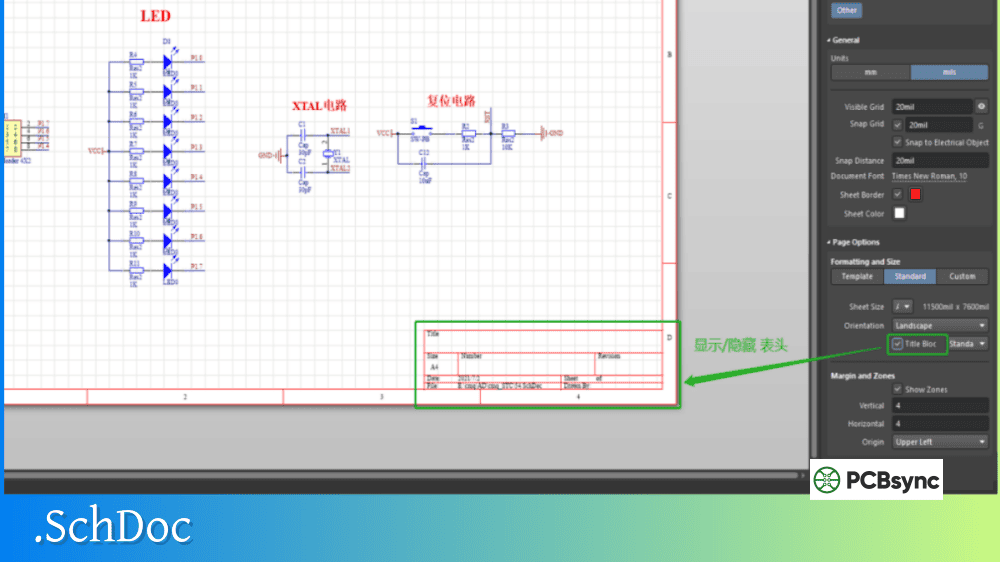
The View Configuration panel controls how your board appears in 3D. Access it through View → Panels → View Configuration or press L.
View Options Tab Settings
Setting
Purpose
Projection
Choose between Perspective (realistic depth) or Orthographic (no depth distortion)
Show 3D Bodies
Toggle display of 3D component models
Board Thickness
Visual representation of PCB substrate
Colors
Layer and mask color configuration
Realistic vs. Performance Display
Altium offers different rendering quality levels. For day-to-day work, the default settings provide good balance between visual quality and performance. When creating presentation renders, you can increase quality settings for more realistic results.
Performance note: Complex designs with many 3D models can slow down navigation. If you’re experiencing lag, try hiding 3D bodies temporarily while working on placement or routing.
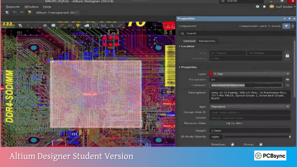
Working with 3D Component Models
The quality of your 3D visualization depends entirely on having accurate 3D models for your components. Without proper models, components appear as simple colored boxes based on their footprint dimensions.
Types of 3D Bodies in Altium
Type
Description
Use Case
Extruded
2D shape pulled to a height
Simple rectangular components
Cylinder
Circular cross-section
Capacitors, standoffs
Sphere
Ball shape
Rarely used for components
Generic (STEP)
Full 3D CAD model
Accurate component representation
Adding STEP Models to Footprints
For the most accurate 3D representation, use STEP models imported into your footprints:
Open the footprint in the PCB Library editor
Select Place → 3D Body
In the Properties panel, set 3D Model Type to Generic
Click Embed STEP Model and select your .step file
Adjust position, rotation, and standoff height as needed
Save the footprint
The STEP model is now embedded in the footprint and will appear whenever that component is placed on a PCB.
Where to Find 3D Models
Finding accurate STEP models used to be a challenge, but several resources now make this much easier:
When downloading models, verify dimensions against the component datasheet. Not all community-contributed models are accurate.
Importing Enclosures and Mechanical Parts
One of the most powerful uses of Altium Designer 3D View is verifying that your board fits in its enclosure. You can import STEP models of enclosures, mounting hardware, and other mechanical parts directly into the PCB editor.
How to Import an Enclosure STEP File
Open your PCB document
Switch to 3D view (press 3)
Select Place → 3D Body
Set 3D Model Type to Generic
Choose Embed Model or Link to Model
Browse to your enclosure STEP file
Position the model relative to your board
Once imported, the enclosure becomes part of your design environment. You can check clearances between components and the enclosure walls, verify connector alignment with panel cutouts, and identify any interference issues.
Embedding vs. Linking Models
Option
Behavior
Best For
Embed Model
STEP stored inside PCB file
Final designs, portability
Link to Model
References external file
Designs with evolving mechanical parts
Linked models update automatically when the source file changes, which is useful during concurrent ECAD-MCAD development.
3D Collision Detection and Clearance Checking
Altium doesn’t just show you a static 3D picture—it actively checks for collisions between components.
Setting Up Component Clearance Rules
The Component Clearance design rule controls 3D collision detection:
Go to Design → Rules
Expand Placement → Component Clearance
Create or modify a rule
Set Minimum Horizontal Clearance and Minimum Vertical Clearance
Enable Show actual violation distances to see exact clearance values
When components violate these rules, Altium highlights them in green (by default) and displays the violation distance.
What Gets Checked
Component clearance uses the actual 3D shape of components when STEP models are present. This means:
Complex shapes that fit within each other won’t trigger false violations
The check considers height, not just 2D footprint overlap
Imported enclosures participate in collision detection
Running 3D Clearance Checks
Collision checking happens automatically when Online DRC is enabled. You can also run a Batch DRC that includes Component Clearance rules to generate a report of all violations.
Measuring Distances in 3D
Sometimes you need exact measurements between 3D objects. The Measure 3D Objects command provides this capability.
How to Measure 3D Distances
In 3D view, select Reports → Measure 3D Objects
Hover over the first object (it highlights in green)
Click to select it
Hover over the second object
Click to complete the measurement
The 3D Distance dialog shows:
Distance in X, Y, and Z planes
Shortest distance between objects
Exact surface-to-surface measurement
Tip: Hold Ctrl while hovering to select a specific face on a 3D object rather than the entire object.
Using Section Views
Sometimes you need to see inside your board—for example, to verify via placement through the layer stack or check components placed under other components.
Enabling Section View
In 3D view, go to View → Toggle Section View (or Shift+Ctrl+V)
The view switches to Edit mode, showing section planes
Click and drag the colored arrows to move section planes
Each color corresponds to an axis (X=red, Y=green, Z=blue)
Section views cut away portions of the board, revealing internal structure. This is particularly useful for:
Inspecting via connections to internal layers
Verifying component placement in cavities
Checking clearances for components mounted under other parts
For detailed examination without leaving your 2D workspace, use the 3D Visualization panel.
Accessing the Panel
Click the PCB button at the bottom-right of Altium Designer
Select 3D Visualization from the menu
The panel displays up to three simultaneous 3D views
Panel Features
View
Purpose
3D Board Insight
Floating view centered on cursor position
Section A-A
Cross-section along X-axis
Section B-B
Cross-section along Y-axis
The panel updates in real-time as you move your cursor in the 2D view, giving you instant 3D context for any area of your design.
Thickness Scaling
The Thickness Scaling slider in the panel multiplies the vertical scale of the board (1x to 100x). This makes it easier to differentiate layers when viewing cross-sections, particularly useful for HDI designs with many layers.
Exporting 3D Views and Models
Once your design is complete, you can export 3D representations for documentation, review, or mechanical integration.
Export Options
Format
Purpose
How to Export
STEP (.step, .stp)
Full 3D model for MCAD
File → Export → STEP 3D
3D Screenshot
High-res image
View → 3D Screenshot
3D Video
Animated flyover
View → 3D Video
PDF 3D
Interactive 3D in PDF
Via Output Job file
STEP Export Options
When exporting STEP files, you can choose:
Export as Single Part: Simplifies the model but loses individual component selection
Include 3D Bodies: Include/exclude component models
Include Pad Holes: Include/exclude drilled holes
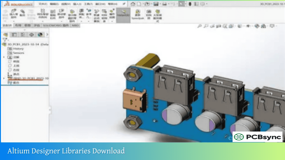
The exported STEP file can be imported into SolidWorks, Fusion 360, or other MCAD tools for mechanical integration.
Troubleshooting Common 3D View Issues
Components Not Appearing in 3D
If components show as blank boxes or don’t appear:
Check that Show 3D Bodies is enabled in View Configuration
Verify the footprint has a 3D body defined
Check the 3D body opacity in the PCB panel (3D Models mode)
Frequently Asked Questions About Altium Designer 3D View
What are the system requirements for 3D visualization in Altium Designer?
You need a graphics card that supports DirectX 9.0c or later and Shader Model 3 or later. Most modern graphics cards meet these requirements. To verify your system compatibility, go to DXP → Preferences → PCB Editor → Display and click the test button. If you’re experiencing problems, ensure DirectX is enabled with the “Use DirectX if possible” option. Integrated graphics on laptops may work but dedicated graphics cards provide significantly better performance, especially for complex designs with many 3D component models.
Why do some components appear as colored boxes instead of 3D models?
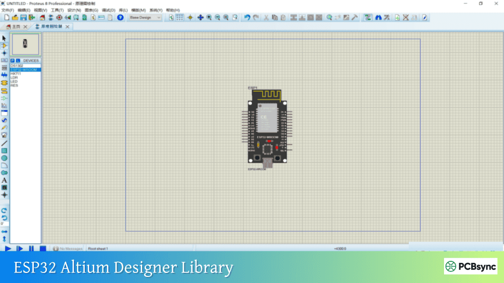
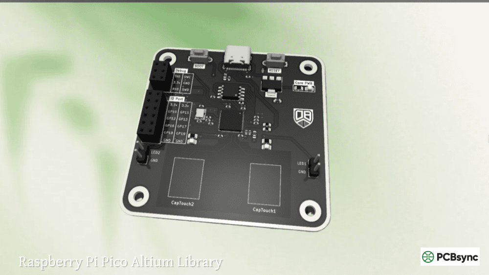
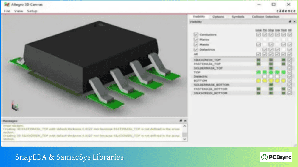
Components appear as simple boxes when their footprints don’t include 3D body definitions. The default behavior creates an extruded box based on the footprint dimensions. To get accurate 3D representation, you need to add STEP models to your footprints—either by downloading pre-made models from sources like SnapEDA or SamacSys, or by creating simple shapes using Altium’s built-in 3D body tools (extruded, cylinder, sphere). Components from Altium’s official libraries typically include 3D models, while older or custom libraries may not.
Can I check if my board fits in the enclosure using Altium Designer?
Yes, this is one of the most valuable uses of Altium’s 3D capabilities. Import your enclosure as a STEP file using Place → 3D Body, then configure Component Clearance design rules to check for interference. Altium will highlight any collisions between your PCB components and the enclosure walls. You can also use the Measure 3D Objects command to verify exact clearances. For more complex scenarios with multiple boards, consider using Altium’s Multi-board Assembly feature, which includes dedicated collision checking between boards and enclosure parts.
How do I export a 3D model of my PCB to share with mechanical engineers?
Go to File → Export → STEP 3D to generate a STEP file of your complete board assembly including all 3D component models. In the export options, choose whether to export as a single part or as an assembly (which allows selecting individual components in MCAD software). The exported STEP file can be imported into SolidWorks, Fusion 360, Inventor, or any other mechanical CAD tool. For simpler sharing, you can also create high-resolution 3D screenshots or generate 3D videos showing board rotation and flyover views.
How do I improve performance when 3D view is slow?
Several approaches can help with sluggish 3D performance. First, ensure your graphics drivers are up to date and that DirectX is enabled in Altium preferences. For complex boards, temporarily hide 3D bodies in the View Configuration panel while you’re not actively checking fit—this significantly improves navigation speed. You can also reduce the number of visible layers or turn off polygon pour display. If you regularly work with complex 3D designs, consider upgrading to a dedicated graphics card rather than relying on integrated graphics, as GPU performance directly impacts 3D rendering speed.
Getting the Most from 3D Visualization
Altium Designer 3D View transforms how you approach PCB design validation. Rather than discovering mechanical conflicts after fabrication—or worse, after assembly—you can catch and resolve these issues during the design phase when changes are cheap and easy.
My recommendation is to make 3D visualization a regular part of your design workflow, not just something you use at the end for pretty pictures. Check your 3D view after component placement to verify heights and clearances. Import enclosure models early in the design process so you’re designing within known constraints from the start. Use collision detection rules to catch problems automatically rather than relying on visual inspection alone.
The initial investment in setting up proper 3D models pays dividends throughout the project lifecycle. When your footprint library includes accurate STEP models, every future design benefits from reliable 3D visualization without additional effort. And when you need to communicate your design to mechanical engineers, manufacturing partners, or clients, having a realistic 3D representation speaks volumes that no 2D drawing ever could.
Take the time to learn the navigation controls and configure your view settings. Once 3D becomes second nature, you’ll wonder how you ever designed boards without it.
Inquire: Call 0086-755-23203480, or reach out via the form below/your sales contact to discuss our design, manufacturing, and assembly capabilities.
Quote: Email your PCB files to Sales@pcbsync.com (Preferred for large files) or submit online. We will contact you promptly. Please ensure your email is correct.
Notes: For PCB fabrication, we require PCB design file in Gerber RS-274X format (most preferred), *.PCB/DDB (Protel, inform your program version) format or *.BRD (Eagle) format. For PCB assembly, we require PCB design file in above mentioned format, drilling file and BOM. Click to download BOM template To avoid file missing, please include all files into one folder and compress it into .zip or .rar format.


