Inquire: Call 0086-755-23203480, or reach out via the form below/your sales contact to discuss our design, manufacturing, and assembly capabilities.
Quote: Email your PCB files to Sales@pcbsync.com (Preferred for large files) or submit online. We will contact you promptly. Please ensure your email is correct.
Notes: For PCB fabrication, we require PCB design file in Gerber RS-274X format (most preferred), *.PCB/DDB (Protel, inform your program version) format or *.BRD (Eagle) format. For PCB assembly, we require PCB design file in above mentioned format, drilling file and BOM. Click to download BOM template To avoid file missing, please include all files into one folder and compress it into .zip or .rar format.
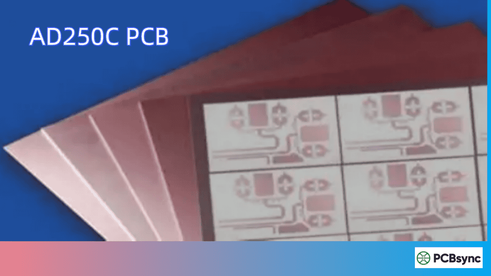
If you’ve been designing RF or microwave circuits for base station antennas, you’ve probably heard about the AD250C laminate. As a PCB engineer who’s worked with dozens of high-frequency materials over the years, I can tell you that AD250C strikes an impressive balance between performance and cost—something that’s hard to find in PTFE-based materials.
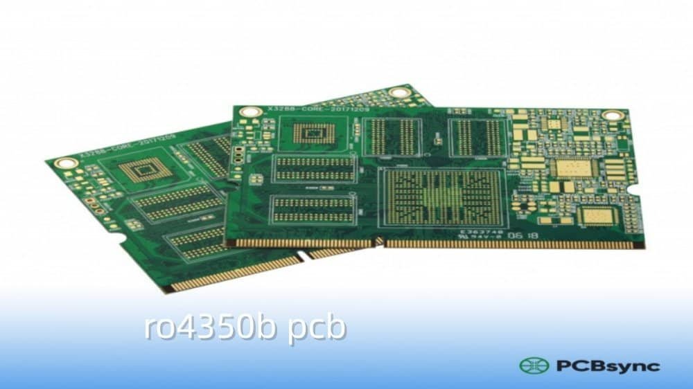
This guide covers everything you need to know about Rogers AD250C: from its technical specifications and real-world applications to practical design tips that’ll save you headaches during fabrication. Whether you’re evaluating AD250C for your next antenna project or comparing it against alternatives like RO4350B, you’ll find the answers here.
Rogers AD250C is a third-generation PTFE/woven fiberglass/ceramic-filled laminate material designed specifically for microwave and RF printed circuit boards. Originally developed by Arlon (now part of Rogers Corporation), AD250C belongs to the AD Series™ antenna materials family.
What makes AD250C stand out is its composite architecture. It combines:
PTFE (Polytetrafluoroethylene) for excellent electrical properties
Woven glass reinforcement for mechanical stability and easier processing
Micro-dispersed ceramic fillers for controlled dielectric constant and thermal stability
This combination delivers low-loss performance (Df = 0.0013 at 10 GHz), tight dielectric constant control (Dk = 2.50 ± 0.04), and excellent passive intermodulation (PIM) characteristics—all at a price point that undercuts many traditional PTFE laminates.
The material was engineered with telecom infrastructure in mind, particularly base station antenna applications where consistent RF performance across temperature cycles is critical.
AD250C Material History
AD250C represents the third generation of commercial PTFE-based RF laminates in the AD Series. Originally developed by Arlon Materials for Electronics (a pioneer in high-frequency laminates since 1958), the AD Series became part of Rogers Corporation’s portfolio in 2015 when Rogers acquired Arlon’s printed circuit board division. This acquisition combined Arlon’s PTFE expertise with Rogers’ global manufacturing and distribution capabilities, making materials like AD250C more accessible worldwide.
The “AD” designation stands for “Advanced Dielectric,” reflecting the material’s position as a premium substrate for demanding antenna applications. Over the years, Arlon and Rogers engineers refined the ceramic filler formulation and glass weave structure to optimize the balance between electrical performance, mechanical stability, and manufacturability.
AD250C Key Technical Specifications
Here’s the complete specification table pulled directly from the Rogers datasheet. I’ve organized it by property type so you can quickly find what you need:
Electrical Properties
Property
AD250C Value
Units
Test Conditions
Dielectric Constant (Process)
2.52
–
23°C @ 50% RH, 10 GHz
Dielectric Constant (Design)
2.50
–
C-24/23/50, 10 GHz
Dissipation Factor (Df)
0.0013
–
23°C @ 50% RH, 10 GHz
Thermal Coefficient of Dk
-117
ppm/°C
0 to 100°C, 10 GHz
Volume Resistivity
4.8 × 10⁸
MΩ-cm
C96/35/90
Surface Resistivity
4.1 × 10⁷
MΩ
C96/35/90
Dielectric Strength
979
V/mil
IPC TM-650 2.5.6.2
PIM Performance
-159 / -163
dBc
43 dBm at 1900 MHz
Thermal Properties
Property
AD250C Value
Units
Test Method
Decomposition Temperature (Td)
>500
°C
5% weight loss
CTE – X axis
47
ppm/°C
-55°C to 288°C
CTE – Y axis
29
ppm/°C
-55°C to 288°C
CTE – Z axis
196
ppm/°C
-55°C to 288°C
Thermal Conductivity
0.33
W/(m·K)
Z-direction
Time to Delamination
>60
minutes
288°C
Mechanical & Physical Properties
Property
AD250C Value
Units
Copper Peel Strength
2.6 N/mm (14.8 lbs/in)
35 μm foil @ 288°C
Flexural Strength (MD/CMD)
60.7 / 44.1
MPa
Moisture Absorption
0.04
%
Density
2.28
g/cm³
Flammability
V-0
UL 94
Dimensional Stability
0.02 / 0.06
mils/inch
Available Thicknesses and Panel Sizes
Standard Thicknesses
Tolerance
Panel Sizes
0.020″ (0.508 mm)
± 0.002″
18″ × 12″, 18″ × 24″
0.030″ (0.762 mm)
± 0.002″
12″ × 18″, 24″ × 18″
0.060″ (1.524 mm)
± 0.003″
12″ × 18″, 24″ × 18″
Copper cladding options: ½ oz (18 μm) and 1 oz (35 μm) electrodeposited or reverse-treated ED copper foil.
Why Choose AD250C? Key Benefits
After working with AD250C on multiple antenna projects, here’s what I appreciate most about this material:
Low Signal Loss at High Frequencies
With a dissipation factor of just 0.0013 at 10 GHz, AD250C minimizes insertion loss in your RF traces. For antenna feed networks operating in the 1.7–2.7 GHz cellular bands, this translates to higher antenna efficiency and better overall system performance.
Excellent PIM Performance
AD250C achieves PIM values as low as -163 dBc when using S1 copper foil. This is crucial for multi-carrier base station antennas where passive intermodulation can cause interference between channels. The low-profile reverse-treated ED copper option further reduces both PIM and conductive losses.
Tight Dielectric Constant Tolerance
The ±0.04 tolerance on dielectric constant (Dk = 2.50) means you can design impedance-controlled traces with confidence. Unlike materials with ±0.10 or larger Dk tolerances, AD250C gives you the repeatability needed for production quantities.
Cost-Effective PTFE Alternative
Let’s be honest—PTFE materials can get expensive. AD250C was specifically designed as a cost-effective option for commercial telecom applications. It delivers PTFE-level RF performance without the premium pricing of materials like RT/duroid 5880 or RO3003.
Standard PCB Process Compatibility
AD250C is compatible with standard PTFE fabrication processes. You don’t need specialized plasma treatment or sodium etch for adhesion—the woven glass reinforcement and ceramic fillers make it easier to drill, plate, and laminate compared to pure PTFE materials.
AD250C Applications in RF and Antenna Design
AD250C was engineered specifically for antenna applications. Based on my experience and industry use cases, here are the primary applications:
Cellular Infrastructure Antennas
This is where AD250C really shines. Base station antenna feed networks, corporate feed structures, and patch antenna elements commonly use AD250C. The material handles the wide frequency range from 700 MHz to 2.7 GHz that modern LTE/5G antennas require.
Commercial Satellite Radio Antennas
SDARS (Satellite Digital Audio Radio Service) and GPS antenna systems benefit from AD250C’s stable electrical properties and weather resistance.
Automotive Telematics
V2X (vehicle-to-everything) communication antennas, GPS modules, and connected car systems increasingly rely on AD250C for its thermal stability during harsh automotive operating conditions.
Digital Audio Broadcasting (DAB)
DAB antenna systems in the 174–240 MHz and 1452–1492 MHz bands use AD250C for its low loss and consistent performance.
Radar Feed Networks
While not as common as antenna applications, AD250C sees use in radar manifold and feed network designs where cost optimization is important.
5G Infrastructure
With the rollout of 5G networks, massive MIMO antenna arrays require low-loss, high-consistency materials for their complex feed structures. AD250C’s tight Dk tolerance ensures phase matching across multiple antenna elements—critical for beamforming performance. Many 5G macro cell antennas operating in sub-6 GHz bands use AD250C for their corporate feed networks.
IoT and M2M Antennas
The Internet of Things explosion has created demand for cost-effective antenna materials. AD250C fits well for industrial IoT gateways, smart city infrastructure, and machine-to-machine communication devices where RF performance matters but budgets are constrained.
AD250C vs Other Rogers Materials: A Practical Comparison
Choosing between Rogers laminates can be confusing. Here’s a side-by-side comparison of AD250C with other commonly considered materials:
Property
AD250C
AD255C
RO4350B
RO4003C
Dielectric Constant (Dk)
2.50
2.55
3.48
3.38
Dissipation Factor (Df)
0.0013
0.0013
0.0037
0.0027
Material Type
PTFE/Glass/Ceramic
PTFE/Glass/Ceramic
Hydrocarbon/Ceramic
Hydrocarbon/Ceramic
CTE-Z (ppm/°C)
196
196
32
46
Processing
PTFE-compatible
PTFE-compatible
FR-4 compatible
FR-4 compatible
Typical Cost
Medium
Medium
Lower
Lower
Best For
Antennas, Low PIM
Antennas
General RF, Power
Low-loss RF
When to Choose AD250C Over RO4350B
Choose AD250C when:
Ultra-low loss is your priority (0.0013 vs 0.0037 Df)
You need excellent PIM performance for multi-carrier systems
Your design requires lower Dk for wider trace geometries
Antenna efficiency is critical
Choose RO4350B when:
FR-4 processing compatibility is important
You need lower Z-axis CTE for multilayer reliability
Cost is your primary concern
General RF applications below 5 GHz
PCB Design Tips for AD250C
Here are practical design guidelines I’ve learned from working with AD250C:
Drilling Considerations
AD250C’s PTFE content means it behaves differently from FR-4 during drilling. Use carbide drill bits designed for PTFE materials. For hole sizes below 0.3 mm, consider laser drilling to avoid excessive burring. Run drilling at slower feed rates than you’d use for epoxy laminates.
Via Plating Preparation
While AD250C doesn’t require sodium etch like pure PTFE, proper surface preparation before electroless copper plating remains important. Most fabricators use plasma treatment to improve copper adhesion on the hole walls. Confirm your fab house has PTFE processing experience.
Impedance Control
When calculating trace widths for 50Ω microstrip lines, use the design Dk of 2.50 (not the process Dk of 2.52). The design value accounts for the actual RF field distribution in your finished circuit. For 0.030″ thick AD250C with 1 oz copper, expect approximately 4.2 mm trace width for 50Ω characteristic impedance.
Hybrid Stackups
AD250C works well in hybrid multilayer constructions where you combine it with FR-4 for non-critical layers. Use appropriate bonding materials—Rogers CuClad or FastRise bondply are good options. Pay attention to CTE matching to prevent delamination during thermal cycling.
Thermal Management
With thermal conductivity of only 0.33 W/(m·K), AD250C isn’t ideal for high-power applications requiring significant heat dissipation. For power amplifier substrates, consider hybrid constructions with metal-backed cores or use higher thermal conductivity materials like RO4835T.
Copper Foil Selection
For antenna applications where PIM is critical, always specify the reverse-treated (RT) ED copper option. Standard ED copper works fine for less demanding applications. The RT foil provides a smoother copper-dielectric interface that reduces both PIM and conductor loss.
Surface Finish Selection
For AD250C boards, ENIG (Electroless Nickel Immersion Gold) works well for most antenna applications requiring wire bonding or where oxidation resistance matters. If cost is a concern and the application allows it, OSP (Organic Solderability Preservative) or immersion tin are alternatives. Avoid HASL (Hot Air Solder Leveling) if you need tight planarity for antenna patches—the uneven surface can affect pattern performance.
Ground Plane Considerations
When designing microstrip antenna elements on AD250C, ensure your ground plane is solid and continuous beneath the radiating patches. Any slots, gaps, or via stitching patterns in the ground can affect antenna characteristics. For feed networks, use adequate via stitching along the edges of coplanar waveguide or grounded coplanar structures to prevent unwanted mode propagation.
Environmental Considerations
AD250C has excellent moisture absorption at just 0.04%—significantly lower than FR-4’s typical 0.15-0.20%. This makes it suitable for outdoor antenna applications. However, for deployments in extreme humidity or direct weather exposure, consider conformal coating or proper radome design to protect the assembled PCB.
Working with PCB Fabricators
A few tips when ordering AD250C boards:
Confirm material availability — AD250C isn’t stocked everywhere. Verify your fabricator has it in inventory or can source it within your lead time.
Provide complete specifications — Include the exact Rogers material designation, thickness, copper weight, and any surface finish requirements in your documentation.
Discuss stackup early — For multilayer designs, collaborate with your fabricator on the stackup design. They may have specific prepreg or bonding material recommendations.
Request impedance coupons — For production quantities, ask for impedance test coupons to verify your trace geometries are achieving target impedance values.
Factor in longer lead times — Specialty materials like AD250C typically have longer lead times than standard FR-4. Plan accordingly.
Useful Resources and Downloads
Here are the essential resources for working with AD250C:
IPC-4103 — Specification for base materials for high-speed/high-frequency applications
IPC-6012 — Qualification and performance specification for rigid PCBs
Frequently Asked Questions
What is the dielectric constant of AD250C?
AD250C has a process dielectric constant (Dk) of 2.52 and a design dielectric constant of 2.50, both measured at 10 GHz. The design value accounts for the actual microstrip field distribution. Use Dk = 2.50 for your impedance calculations.
Is AD250C compatible with lead-free soldering?
Yes. AD250C has a decomposition temperature (Td) exceeding 500°C and time-to-delamination greater than 60 minutes at 288°C. It easily withstands lead-free reflow profiles with peak temperatures around 260°C.
What’s the difference between AD250C and AD255C?
Both materials share similar loss characteristics (Df = 0.0013), but AD255C has a slightly higher dielectric constant (2.55 vs 2.50). AD255C also offers more thickness options including 0.040″ and 0.125″ versions. Choose based on your required Dk and available thicknesses.
Can AD250C be used in multilayer PCBs?
Absolutely. AD250C is commonly used in multilayer constructions for antenna feed networks. Its low Z-axis thermal expansion (compared to pure PTFE materials) improves plated through-hole reliability. Use compatible bonding materials and work with a fabricator experienced in PTFE multilayer processing.
How does AD250C compare to FR-4 for RF applications?
AD250C significantly outperforms FR-4 at high frequencies. At 10 GHz, AD250C’s dissipation factor (0.0013) is roughly 15× lower than FR-4 (~0.020). AD250C also provides tighter Dk tolerance and much lower moisture absorption. For any application above 1 GHz where loss matters, AD250C is the better choice.
Conclusion
Rogers AD250C occupies a valuable niche in the RF laminate landscape. It delivers PTFE-level electrical performance with better processability and lower cost than many traditional microwave materials. For base station antennas, commercial wireless systems, and other telecom infrastructure applications, AD250C provides the right balance of low loss, excellent PIM, and practical manufacturing.
The key is understanding where AD250C fits in your design requirements. If ultra-low loss and PIM performance are priorities—and you can accommodate PTFE-style fabrication processes—AD250C deserves serious consideration. For general RF work where FR-4 process compatibility matters more, the RO4000 series remains a strong alternative.
Whatever direction you choose, I hope this guide helps you make an informed decision. Feel free to consult the Rogers technical resources linked above, and don’t hesitate to engage with your PCB fabrication partner early in the design process.
Inquire: Call 0086-755-23203480, or reach out via the form below/your sales contact to discuss our design, manufacturing, and assembly capabilities.
Quote: Email your PCB files to Sales@pcbsync.com (Preferred for large files) or submit online. We will contact you promptly. Please ensure your email is correct.
Notes: For PCB fabrication, we require PCB design file in Gerber RS-274X format (most preferred), *.PCB/DDB (Protel, inform your program version) format or *.BRD (Eagle) format. For PCB assembly, we require PCB design file in above mentioned format, drilling file and BOM. Click to download BOM template To avoid file missing, please include all files into one folder and compress it into .zip or .rar format.


