Inquire: Call 0086-755-23203480, or reach out via the form below/your sales contact to discuss our design, manufacturing, and assembly capabilities.
Quote: Email your PCB files to Sales@pcbsync.com (Preferred for large files) or submit online. We will contact you promptly. Please ensure your email is correct.
Notes: For PCB fabrication, we require PCB design file in Gerber RS-274X format (most preferred), *.PCB/DDB (Protel, inform your program version) format or *.BRD (Eagle) format. For PCB assembly, we require PCB design file in above mentioned format, drilling file and BOM. Click to download BOM template To avoid file missing, please include all files into one folder and compress it into .zip or .rar format.
Acid Traps in PCB Design: What They Are & How to Avoid Them
One of the first design rules I learned as a junior PCB engineer was simple: avoid acute angles in your traces. No angles less than 90 degrees. Use 45-degree routing. The reason given was always the same—acid traps. Fifteen years later, I still follow this guideline, though the manufacturing landscape has changed dramatically. Understanding what acid traps in PCB design actually are, why they matter, and how modern fabrication has evolved helps you make informed decisions about when this rule is critical and when it’s simply good practice.
Acid traps are geometric features in your PCB layout where etching chemicals can accumulate and pool during the fabrication process. When traces meet at acute angles (less than 90 degrees), or when small enclosed spaces form between traces, pads, and vias, these areas can trap the corrosive chemicals used to remove unwanted copper from the board.
The trapped etchant continues working on the copper long after the rest of the board has been properly processed. This over-etching can erode through the trace, creating opens, weak connections, or complete circuit failures. The term “acid trap” comes from the acidic etchants historically used in PCB manufacturing, though the problem exists with any chemical etching process.
How Acid Traps Form During PCB Manufacturing
To understand acid traps, you need to understand the PCB etching process. Contrary to what it might look like, copper traces aren’t drawn onto a blank board. They’re revealed by removing unwanted copper from a fully copper-clad substrate.
Start with a fiberglass substrate fully covered in copper
Apply etch-resistant material (photoresist or toner) to protect desired traces
Expose the board to chemical etchant that dissolves unprotected copper
Rinse away etchant and remove the protective layer
The remaining copper forms your circuit traces
When etchant gets trapped in a corner or pocket, it can’t be properly rinsed away. It continues dissolving copper underneath the protective layer, tunneling into traces that should have been preserved.
Common Etchants and Their Behavior
Etchant Type
Characteristics
Acid Trap Risk
Ferric Chloride (FeCl₃)
Most common DIY etchant, slow, affordable
High
Ammonium Persulfate
Faster than ferric chloride, clear solution
High
Cupric Chloride
Regenerative, used in production
Moderate
Alkaline Etchants
Modern production standard
Lower
Photo-activated
Activates only under UV light
Lowest
Traditional acidic etchants create the highest risk of acid trap problems. Modern photo-activated and alkaline etching processes have significantly reduced—though not eliminated—these concerns.
Common Causes of Acid Traps in PCB Layout
Several design patterns create conditions where etchant can accumulate:
Acute Angle Trace Junctions
The most common cause of acid traps PCB designers encounter is traces meeting at angles less than 90 degrees. The sharp corner creates a pocket where etchant pools and continues etching.
Angle Type
Risk Level
Recommendation
Acute angles (< 45°)
Very High
Avoid completely
45° to 89° angles
High
Avoid when possible
90° angles
Moderate
Acceptable but not ideal
135° angles (45° routing)
Low
Preferred standard
Curved/arc routing
Lowest
Best for high-speed
T-Junctions Without Teardrops
When a trace connects to a pad or another trace at a perpendicular junction, the sharp internal corners can trap etchant. Adding teardrops—gradual copper transitions—eliminates these sharp internal angles.
Tight Spacing Between Features
Even without acute angles, spacing that’s too tight between traces, pads, and vias creates narrow channels where etchant can’t flow freely. These enclosed areas become traps. The minimum spacing depends on your fabricator’s capabilities, but 3 mils (0.076mm) is a common lower limit.
Copper Islands and Slivers
Small, isolated copper features or thin copper “slivers” can act as traps. These features may also detach during etching and float to other areas of the board, causing shorts. Modern design rules flag features narrower than 4 mils as potential problems.
Problems Caused by Acid Traps
When acid traps occur, they create several failure modes:
Problem
Description
Severity
Open circuits
Trace eroded completely through
Critical
Weak connections
Partially eroded trace with reduced cross-section
High
Via damage
Acid travels through via to internal layers
High
Solder mask damage
Etchant attacks mask, causing oxidation
Moderate
Intermittent failures
Connection works initially, fails under stress
Difficult to diagnose
The most insidious problem is the weak connection that passes initial testing but fails in the field. A trace that’s been partially eroded might have enough copper to conduct under ideal conditions but fails under thermal stress or vibration.
Design Techniques to Avoid Acid Traps
Preventing acid traps requires attention during layout. These techniques eliminate or minimize the geometric conditions that trap etchant:
Use 45-Degree Routing
The simplest and most effective prevention is routing with 45-degree angles instead of 90-degree turns. Most PCB design tools default to this routing style.
Implementation: When changing trace direction, use two 45-degree bends instead of one 90-degree turn. This eliminates acute internal angles entirely.
Add Teardrops at Junctions
Teardrops are gradual copper transitions between traces and pads or vias. They eliminate the sharp corners that form at T-junctions.
Implementation: Most EDA tools include automatic teardrop insertion. Enable this feature globally and verify that teardrops are applied to all pad and via connections.
Maintain Adequate Spacing
Don’t design to your fabricator’s absolute minimum capabilities unless space constraints demand it. Leave margin for etchant flow.
Recommended Minimums:
Trace-to-trace: 5 mils (0.127mm) or greater
Trace-to-pad: 5 mils minimum
Via-to-via: 8 mils minimum
Avoid grouping vias in tight clusters near traces
Eliminate Copper Islands
Review copper pours for small, isolated areas that might trap etchant or detach during fabrication. Most DFM tools flag copper islands below a minimum size threshold.
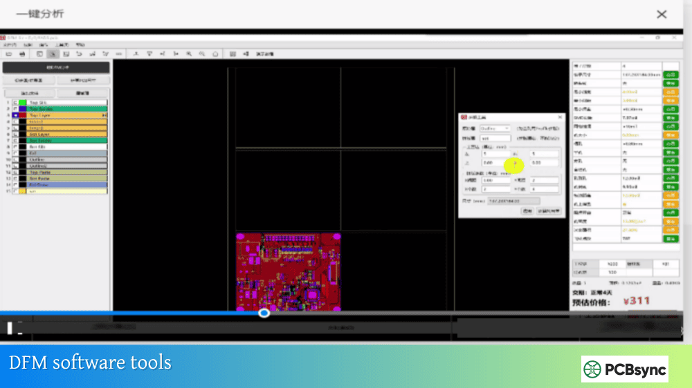
Run DFM Analysis
Design Rule Checking (DRC) catches many issues, but dedicated Design for Manufacturing (DFM) analysis specifically identifies acid trap risks that basic DRC might miss.
Modern Manufacturing: Are Acid Traps Still a Problem?
The PCB industry has evolved significantly, and modern fabrication processes have greatly reduced acid trap risks:
Photoresist Technology
Modern photoresist provides uniform, high-quality coverage that’s far more resistant to etchant penetration than older methods. UV-hardened resist creates a robust barrier that prevents tunneling even when etchant pools briefly.
Alkaline and Photo-Activated Etchants
Most production PCB facilities have moved away from traditional acidic etchants. Alkaline etching solutions are less aggressive and more controllable. Photo-activated etchants only work when exposed to UV light, providing precise control over where etching occurs.
Improved Process Control
Modern spray etching systems ensure etchant is continuously moving across the board surface, preventing pooling. Automated rinsing removes residual chemicals before they can cause damage.
The Practical Reality
Does this mean you can ignore acid traps entirely? Not quite. While modern manufacturing has dramatically reduced the risk, following good design practices costs nothing and provides margin against process variations. Some fabricators—particularly lower-cost offshore suppliers or DIY processes—may still use older methods where acid traps are more problematic.
The recommendation: continue using 45-degree routing and avoiding acute angles as standard practice. It’s become an industry convention that ensures compatibility across fabricators and provides design margin without any real cost.
IPC-2221: Generic standard on printed board design
IPC-2222: Sectional design standard for rigid organic boards
IPC-7351: Land pattern requirements
Manufacturer Resources
Most PCB fabricators publish design guidelines that include angle and spacing recommendations. Request your fabricator’s design rules before starting layout.
Frequently Asked Questions About Acid Traps in PCB Design
Are 90-degree trace angles really a problem?
For acid traps specifically, 90-degree angles are borderline—they create potential pooling areas but aren’t as problematic as acute angles. The bigger concern with 90-degree angles is signal integrity in high-speed designs, where the extra capacitance at corners can cause reflections. Using 45-degree routing eliminates both concerns with no downside, making it the preferred standard. Modern etching processes handle 90-degree angles reasonably well, but there’s no reason to use them when 45-degree routing is equally easy.
Do I need to worry about acid traps with a reputable PCB manufacturer?
Reputable manufacturers using modern processes have largely eliminated acid trap problems through improved etchants and process control. However, designing to avoid acid traps costs nothing and provides margin against process variations. It also ensures your design works if you later switch to a different fabricator or need to use a lower-cost supplier. Consider it cheap insurance that’s already built into standard design practices.
Can DRC catch all acid trap issues?
Basic Design Rule Checking catches acute angles if you’ve configured angle rules, but it may miss more subtle acid trap conditions like tight enclosed spaces or problematic copper pour geometries. Dedicated DFM analysis tools provide more comprehensive checking. Running both DRC and DFM analysis before release gives you the best coverage. Many fabricators offer free DFM checking as part of their service.
What angle should I use for PCB routing?
Use 45-degree routing as your default for all designs. This creates 135-degree corners when changing direction—smooth transitions that eliminate acid trap risk and provide good signal integrity. For very high-speed designs (multi-gigabit signals), curved arc routing provides even smoother transitions. Avoid angles less than 90 degrees entirely, and use 90-degree angles only when absolutely necessary for space constraints.
How do teardrops help prevent acid traps?
Teardrops eliminate the sharp internal corners that form where traces connect to pads and vias. Without teardrops, these T-junctions create exactly the kind of acute internal angles that trap etchant. With teardrops, the copper transitions gradually, eliminating the pocket where chemicals could accumulate. Most PCB design tools can automatically insert teardrops—enable this feature globally for best results.
Conclusion: Good Practice That Costs Nothing
Acid traps represent a historical concern that modern manufacturing has largely addressed. But the design practices developed to prevent them—45-degree routing, adequate spacing, teardrops, DFM analysis—remain valuable because they cost nothing to implement and provide margin against manufacturing variations. They’ve become industry conventions that every PCB designer should follow.
Whether you’re designing a simple two-layer board or a complex HDI stack-up, using 45-degree routing and avoiding acute angles ensures your design is manufacturable across the widest range of fabricators. It’s one of those best practices that’s easy to follow and has no downside—the definition of a design rule worth keeping.
Inquire: Call 0086-755-23203480, or reach out via the form below/your sales contact to discuss our design, manufacturing, and assembly capabilities.
Quote: Email your PCB files to Sales@pcbsync.com (Preferred for large files) or submit online. We will contact you promptly. Please ensure your email is correct.
Notes: For PCB fabrication, we require PCB design file in Gerber RS-274X format (most preferred), *.PCB/DDB (Protel, inform your program version) format or *.BRD (Eagle) format. For PCB assembly, we require PCB design file in above mentioned format, drilling file and BOM. Click to download BOM template To avoid file missing, please include all files into one folder and compress it into .zip or .rar format.


