Inquire: Call 0086-755-23203480, or reach out via the form below/your sales contact to discuss our design, manufacturing, and assembly capabilities.
Quote: Email your PCB files to Sales@pcbsync.com (Preferred for large files) or submit online. We will contact you promptly. Please ensure your email is correct.
Notes: For PCB fabrication, we require PCB design file in Gerber RS-274X format (most preferred), *.PCB/DDB (Protel, inform your program version) format or *.BRD (Eagle) format. For PCB assembly, we require PCB design file in above mentioned format, drilling file and BOM. Click to download BOM template To avoid file missing, please include all files into one folder and compress it into .zip or .rar format.
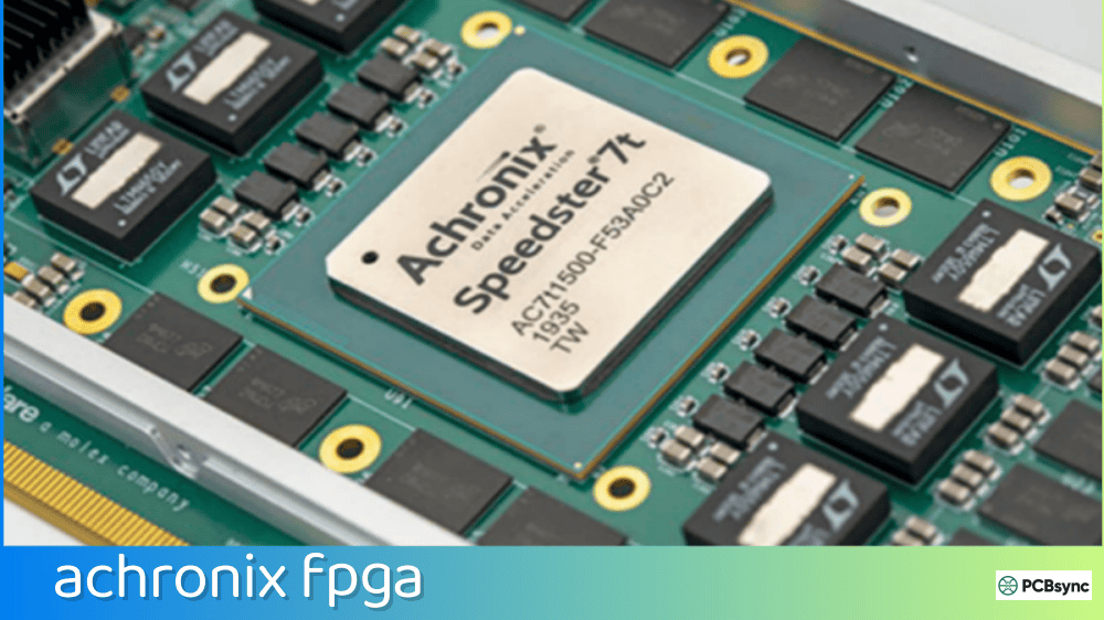
When I first encountered Achronix FPGA devices about three years ago while working on a high-speed networking project, I was honestly skeptical. Another FPGA vendor trying to compete with the Xilinx-Intel duopoly? My team and I had been burned before by smaller vendors who couldn’t deliver on their promises. But Achronix changed my perspective entirely.
Achronix Semiconductor Corporation, founded in 2004 and headquartered in Santa Clara, California, has carved out a unique position in the FPGA market. They’re the only high-end FPGA manufacturer that also offers embedded FPGA (eFPGA) IP solutions. This dual approach—standalone Speedster7t FPGAs and licensable Speedcore eFPGA IP—gives designers unprecedented flexibility in their product roadmaps.
What makes Achronix FPGA technology particularly compelling for PCB engineers is the seamless migration path. You can prototype and validate your design on a Speedster7t FPGA, then transition the same RTL code to a custom ASIC with embedded Speedcore eFPGA when you’re ready for high-volume production. That’s a significant advantage that the other big players simply can’t match.
The Speedster7t family represents Achronix’s flagship FPGA product line, built on TSMC’s 7nm FinFET process technology. These devices are specifically engineered for high-bandwidth data acceleration applications where traditional FPGAs hit performance walls.
Revolutionary 2D Network-on-Chip (2D NoC)
The defining feature of any Achronix FPGA in the Speedster7t family is the two-dimensional Network-on-Chip (2D NoC). Having implemented designs on both traditional FPGA fabrics and the Speedster7t architecture, I can tell you the difference is night and day.
Traditional FPGAs force you to route wide data buses through the programmable interconnect fabric. When you’re dealing with 400G Ethernet—which requires a 1024-bit internal bus running at 724 MHz—that becomes essentially impossible with conventional FPGA routing. The Speedster7t’s 2D NoC solves this problem elegantly.
The 2D NoC provides over 20 Tbps of total on-chip bandwidth through dedicated routing channels that operate independently of the FPGA fabric. Each row and column in the NoC features two 256-bit, unidirectional AXI4-compatible channels running at 512 Gbps in each direction. The NoC connects to over 80 access points distributed throughout the FPGA fabric.
From a practical standpoint, this architecture delivers a 40% reduction in logic resources compared to traditional FPGA routing, with compile times reduced by approximately 40% as well. The NoC essentially creates a superhighway for data movement that sits above the programmable logic fabric.
Machine Learning Processors (MLPs)
Achronix FPGA devices include specialized Machine Learning Processor (MLP) blocks distributed throughout the fabric. Each MLP contains 32 multiplier/accumulator (MAC) units that support various data formats:
Integer formats from 4-bit to 24-bit precision
TensorFlow’s bfloat16 floating-point format (native support)
Block floating-point (BFP) format for efficient AI inference
16-bit half-precision floating-point
The MLPs include a cyclical register file that leverages temporal locality for weight and data reuse, significantly reducing data movement overhead. The top-end Speedster7t AC7t1500 device can achieve up to 134 TOPS on INT8 operations when utilizing both the MLPs and fabric-based multipliers.
Speedster7t Family Specifications Comparison
Feature
AC7t800
AC7t1500
Key Benefits
Logic (LUT6)
~800K
~1.5M
High-density designs
2D NoC Bandwidth
12 Tbps
20+ Tbps
ASIC-like routing
SerDes Speed
Up to 112 Gbps
Up to 112 Gbps
Industry-leading
Ethernet
2x 400GE
2x 400GE
Hard IP MACs
PCIe
Gen5 x16
Gen5 x16
64 GT/s per lane
GDDR6 Channels
6 channels
8 channels
Up to 4 Tbps total
DDR Support
DDR4/DDR5
DDR4/DDR5
DFI 4.0 compliant
Process Node
TSMC 7nm
TSMC 7nm
Power efficiency
High-Speed Interface Support
From a PCB design perspective, the Speedster7t’s interface portfolio is comprehensive. The devices include hard IP for all major high-speed interfaces, which means lower power consumption and more predictable timing compared to soft IP implementations.
400G Ethernet Capabilities
Each Speedster7t device includes two 400G Ethernet MAC blocks with highly flexible port configurations. The MACs support SerDes lane rates from 10 Gbps to 100 Gbps, enabling various Ethernet configurations including 4x100GE, 8x50GE, or 16x25GE. The high-performance Ethernet interfaces connect directly to the 2D NoC for maximum throughput.
PCIe Gen5 Integration
PCIe Gen5 support at x16 configuration provides 64 GT/s per lane—crucial for data center accelerator card applications. The PCIe controller is fully integrated with the NoC, enabling seamless data movement between the host system and FPGA fabric or external memory interfaces.
GDDR6 Memory Interface
Perhaps the most distinctive feature of the Achronix FPGA Speedster7t family is native GDDR6 support. Each GDDR6 controller provides 512 Gbps of bandwidth, and with up to 8 controllers in the AC7t1500, you get 4 Tbps of aggregate memory bandwidth. This is comparable to HBM-equipped FPGAs but at significantly lower cost and PCB complexity.
For board designers, GDDR6 is much more straightforward to implement than HBM. You’re dealing with standard BGA packages on a multi-layer PCB rather than silicon interposer technology. The DDR5 interfaces provide additional flexibility for deeper buffering requirements, supporting UDIMM, SODIMM, RDIMM, and LRDIMM configurations.
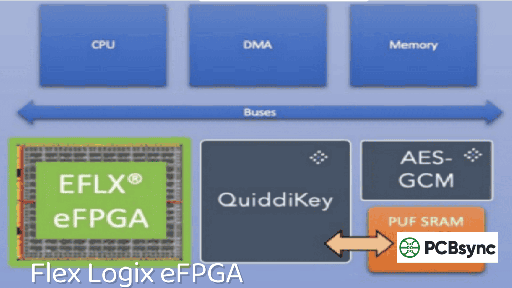
Speedcore eFPGA IP: Embedded FPGA for Custom Silicon
The Speedcore eFPGA IP represents Achronix’s embedded FPGA offering—licensable IP that integrates directly into custom ASICs and SoCs. This is where the company’s unique value proposition really shines.
Understanding eFPGA Technology
An eFPGA is fundamentally an FPGA IP block that gets integrated into your custom silicon during the ASIC design process. Unlike a standalone FPGA, you specify exactly the resources you need—the number of LUTs, memory blocks, DSP units, and I/O connections.
The key advantage is eliminating the overhead of a standalone FPGA. You’re not paying for unused I/O, package pins, or logic resources. The eFPGA becomes part of your ASIC’s die, sharing power supplies and operating at ASIC-typical frequencies in the surrounding logic while the programmable fabric runs at FPGA speeds (typically 300-500 MHz).
Speedcore Architecture Components
Speedcore eFPGA IP uses the same architectural elements as the Speedster7t FPGAs, ensuring code portability. Available building blocks include:
Logic: 6-input LUTs implementing up to 7-input functions in a single logic level
Logic RAM: LRAM2k (2 kb) and LRAM4k (4 kb) blocks
Block RAM: BRAM72k (72 kb with ECC) and BRAM20k (20 kb) blocks
DSP64: 18×27 multiplier with 64-bit accumulator and 27-bit pre-adder
MLP: 32 MAC units per block, supporting integer and floating-point formats
2D NoC: Scalable network-on-chip for high-bandwidth data movement
Speedcore eFPGA vs Standalone FPGA Comparison
Aspect
Standalone FPGA
Speedcore eFPGA
Resource Allocation
Fixed by device SKU
Customer-defined exact amounts
Board Space
Separate package required
Integrated into SoC die
Power Consumption
Higher (I/O, package overhead)
Up to 50% reduction
Cost at Volume
Higher unit cost
Up to 90% cost reduction
Performance
FPGA fabric speeds
10X throughput improvement
Scale Range
Limited SKU options
<10K to >1M LUTs
Process Technology
Vendor-determined
TSMC 7nm, 12FFC, 16FF+
Speedcore Integration Workflow
The Speedcore integration process follows a structured methodology that aligns with standard ASIC design flows:
Benchmark Phase: Run target designs through ACE tools to determine required programmable resources
Sizing: Achronix provides die size and aspect ratio based on benchmark results and target process
Licensing: Standard contract defines operating conditions, dimensions, resource counts, and specifications
Delivery: Achronix delivers GDSII files for integration plus custom ACE tools for programming
ASIC Integration: Customer integrates eFPGA into their ASIC design using standard EDA flows
A critical consideration: ASIC logic typically operates above 1 GHz while FPGA fabric runs at 300-500 MHz. Plan your clock domain crossings carefully at the eFPGA boundary. Achronix has shipped over 10 million Speedcore eFPGA IP cores to date, demonstrating the technology’s production maturity.
Achronix FPGA Applications and Use Cases
The combination of high-bandwidth interfaces, ML processing capability, and the 2D NoC makes Achronix FPGA devices well-suited for several demanding application areas.
Artificial Intelligence and Machine Learning Acceleration
AI inference workloads benefit significantly from the Speedster7t architecture. The distributed MLP blocks, combined with high-bandwidth GDDR6 memory, enable efficient execution of neural network models. Unlike GPUs that require large batch sizes due to their SIMD architecture, FPGAs can execute multiple parallel pipelines simultaneously, making them ideal for low-latency inference.
Achronix has demonstrated solutions for automatic speech recognition (ASR) that process over 1,000 concurrent real-time streams with 20X performance improvement over competing GPU solutions. The FPGA-based approach delivers up to 16X better performance-to-cost ratio for ASR workloads.
5G/6G Wireless Infrastructure
Wireless infrastructure represents a natural fit for Achronix FPGA technology. The Speedster7t devices support virtualized distributed unit (DU) and central unit (CU) acceleration through the VectorPath accelerator platform. The Achronix Network Infrastructure Code (ANIC) framework provides kernel-mode drivers for workload offloading.
Key wireless capabilities include signal processing kernel acceleration, ADC/DAC interfacing, real-time beamforming, and security protocol implementation. The eFPGA approach also allows semiconductor suppliers to integrate custom amounts of programmable logic into their baseband processors.
Data Center Networking and SmartNICs
The explosion of data center traffic driven by SDN, Open vSwitch, and NFV demands programmable network acceleration. Speedster7t devices uniquely support Terabit Ethernet switching—a capability that traditional FPGAs simply cannot achieve due to routing limitations.
For SmartNIC implementations, the combination of 400G Ethernet, PCIe Gen5, and GDDR6 memory provides a wire-speed flexible architecture. Applications include packet processing acceleration, traffic management, data-path security, and DPU implementations.
High-Frequency Trading
The financial trading sector demands the lowest possible latency. Unlike Intel’s chiplet-based approach (which adds latency to transceiver paths), Speedster7t devices maintain direct connections between SerDes and fabric, minimizing end-to-end latency for market data processing and order execution.
ACE Design Tools and Development Environment
The Achronix Tool Suite centers on ACE (Achronix CAD Environment), which handles placement, routing, timing analysis, and bitstream generation. The toolchain integrates with industry-standard EDA tools.
Toolchain Components
ACE: Place and route, timing analysis, bitstream generation, I/O Designer
Synplify Pro: Achronix-optimized version from Synopsys for synthesis
The I/O Designer tool deserves special mention—it provides real-time configuration and design rule checking for all I/O types including GPIO, PCIe, Ethernet, raw SerDes, 2D NoC, GDDR6, and DDR5. For engineers migrating from Xilinx or Intel platforms, the Synplify Pro-based synthesis flow simplifies the transition since many designers already have experience with this tool.
Achronix has documented the migration process for designs coming from Xilinx and Intel platforms. Key considerations include:
Standard RTL (VHDL/Verilog) requires minimal changes
Synplify Pro handles LUT and register inference automatically
Memory and DSP inference works with standard templates
I/O constraints require conversion (ACE uses separate constraint files)
Vendor-specific primitives need replacement with Achronix equivalents
PCB Design Considerations for Achronix FPGA
As a PCB engineer, you’ll appreciate that Achronix provides comprehensive board design guidance. The AC7t1500 Board Designers Guide covers critical aspects of high-speed design.
High-Speed Interface Routing
With SerDes running up to 112 Gbps, signal integrity is paramount. Key considerations include:
Minimal via stubs—consider via-in-pad or back-drilling
Length matching for differential pairs
Reference plane continuity under high-speed signals
Power Distribution
Speedster7t devices require multiple power rails. Work closely with your power management IC vendor—Achronix has partnered with companies like Monolithic Power Systems for reference designs. Key voltage rails include core supply, I/O banks, and SerDes power domains.
Memory Interface Layout
GDDR6 interfaces require careful attention to trace routing symmetry and termination. DDR5 support includes configurations for soldered components, UDIMM, SODIMM, RDIMM, and LRDIMM. The PHY interface is DFI 4.0 compliant, allowing flexibility in controller implementation.
Useful Resources and Documentation
The following resources will help you get started with Achronix FPGA development:
Developed jointly with BittWare: Data center-class evaluation and production platform
Frequently Asked Questions About Achronix FPGA
1. How does Achronix FPGA compare to Xilinx and Intel FPGAs?
Achronix Speedster7t devices compete directly with Xilinx Versal and Intel Agilex families. All three use advanced process nodes (TSMC 7nm or Intel 10nm). Achronix differentiates through its 2D NoC architecture, native GDDR6 support (versus HBM in competitors), and the unique ability to migrate designs to eFPGA IP for high-volume production. The Speedster7t family leads in raw LUT count, with the AC7t1500 offering approximately 1.5M LUT6-equivalents. For bandwidth-intensive applications like 400G networking, Achronix’s NoC architecture provides advantages that traditional FPGA routing cannot match.
2. What is the advantage of GDDR6 over HBM memory in FPGAs?
GDDR6 offers comparable bandwidth (4 Tbps aggregate with 8 channels) to HBM-based solutions but with significant practical advantages. From a PCB design standpoint, GDDR6 uses standard BGA packaging on conventional multi-layer boards, while HBM requires silicon interposer technology. This translates to lower manufacturing costs, simpler PCB fabrication, and more accessible component sourcing. For many data center applications, GDDR6 provides the sweet spot of high bandwidth at reasonable cost and complexity.
3. Can I migrate my existing FPGA design to Achronix?
Yes, migration from Xilinx or Intel platforms is well-documented. Standard RTL (VHDL/Verilog) typically requires minimal changes since Synplify Pro handles inference for LUTs, registers, memories, and DSP blocks. The main effort involves converting constraint files (timing and I/O) and replacing any vendor-specific primitives. Achronix provides migration guides with suggested device equivalents based on comparable resources. The I/O assignment flow is more aligned with Intel’s approach, which may ease migration from that platform.
4. What makes Speedcore eFPGA different from competing eFPGA solutions?
Speedcore uses the same silicon-proven architecture as Speedster7t FPGAs. This means you can prototype on a standalone Speedster7t device and migrate to Speedcore eFPGA IP with minimal code changes—the logic structures, memory blocks, and DSP/MLP units are identical. Competing eFPGA solutions require you to port your FPGA code to a different architecture using new tools and optimization strategies. Speedcore also includes advanced features like the 2D NoC and MLP blocks that aren’t available from other eFPGA vendors. With over 10 million cores shipped, Speedcore is production-proven at scale.
5. Is Achronix FPGA suitable for AI inference applications?
Absolutely. The Speedster7t architecture was designed with AI/ML workloads in mind. The distributed MLP blocks support INT4 through INT24 formats plus bfloat16 and block floating-point, giving you flexibility to trade precision versus performance. The high-bandwidth GDDR6 memory eliminates the memory wall that limits many AI accelerators. Unlike GPUs that require large batch sizes, FPGAs can run multiple parallel inference pipelines with low latency—critical for real-time applications like speech recognition or autonomous systems. Achronix has demonstrated 16X better performance-to-cost ratios compared to GPU solutions for certain workloads.
Security Features in Achronix FPGA
In today’s threat landscape, bitstream security is non-negotiable for production deployments. Achronix has implemented multiple layers of defense in the Speedster7t family.
The security architecture includes keys encrypted using a tamper-resistant Physically Unclonable Function (PUF). Bitstreams themselves are encrypted and authenticated using 256-bit AES-GCM. To defend against side-channel attacks, bitstreams are segmented with separately derived keys for each segment, and the decryption hardware employs differential power analysis (DPA) countermeasures.
A 2048-bit RSA public key authentication protocol activates the decryption and authentication hardware. When you load a secure bitstream, it undergoes verification through RSA public key, AES-GCM private key, and CRC checksum—providing confidence that only authorized configurations can be loaded.
Achronix FPGA Market Position and Industry Recognition
While Achronix holds a smaller market share compared to AMD (Xilinx) and Intel in the overall FPGA market, they’ve established meaningful presence in specific high-value segments. According to industry analysts, Achronix holds approximately 1.7% of the enterprise FPGA market share, with notable customer deployments at companies like CERN, Alibaba Cloud, SK Telecom, and Ethernity Networks.
The company’s participation in initiatives like the Open Compute Project demonstrates their commitment to data center standardization. Speedcore eFPGA IP is now recognized as a viable technology for chiplet architectures and system-in-package designs.
Achronix has secured fab capacity and packaging inventory to maintain shorter lead times than competitors—a significant advantage during the ongoing semiconductor supply constraints. For customers starting new designs or looking to redesign existing programs, Speedster7t availability is generally better than competing high-end FPGAs.
Conclusion: Is Achronix FPGA Right for Your Project?
After spending considerable time evaluating and implementing designs on Achronix FPGA platforms, I can say they’ve earned their place in the high-end FPGA market. The Speedster7t family addresses real pain points that we’ve struggled with on other platforms—particularly around high-bandwidth data movement and AI acceleration.
The 2D NoC architecture is genuinely innovative. It’s not just marketing fluff—the ability to route multi-hundred-gigabit data streams without consuming programmable routing resources fundamentally changes what’s achievable in an FPGA. For 400G Ethernet applications or multi-Terabit switching, this capability is practically essential.
The FPGA-to-eFPGA migration path is Achronix’s strongest differentiator. If you’re building products that will eventually move to high-volume production, starting with Speedster7t and planning a transition to Speedcore makes strategic sense. You maintain programmability where you need it while achieving ASIC-like cost and power for the rest of your design.
That said, Achronix is a smaller company than AMD (Xilinx) or Intel. If your priority is extensive ecosystem support, third-party IP availability, or having local field application engineers in every region, the larger vendors may better fit your needs. But for performance-focused designs in networking, AI acceleration, or 5G infrastructure, Achronix FPGA technology deserves serious consideration.
The VectorPath accelerator card provides an accessible entry point for evaluation. I’d recommend requesting an evaluation license for ACE tools and running your target application through the flow. The performance numbers Achronix claims are achievable in practice—I’ve validated them on my own projects.
Inquire: Call 0086-755-23203480, or reach out via the form below/your sales contact to discuss our design, manufacturing, and assembly capabilities.
Quote: Email your PCB files to Sales@pcbsync.com (Preferred for large files) or submit online. We will contact you promptly. Please ensure your email is correct.
Notes: For PCB fabrication, we require PCB design file in Gerber RS-274X format (most preferred), *.PCB/DDB (Protel, inform your program version) format or *.BRD (Eagle) format. For PCB assembly, we require PCB design file in above mentioned format, drilling file and BOM. Click to download BOM template To avoid file missing, please include all files into one folder and compress it into .zip or .rar format.


