Inquire: Call 0086-755-23203480, or reach out via the form below/your sales contact to discuss our design, manufacturing, and assembly capabilities.
Quote: Email your PCB files to Sales@pcbsync.com (Preferred for large files) or submit online. We will contact you promptly. Please ensure your email is correct.
Notes: For PCB fabrication, we require PCB design file in Gerber RS-274X format (most preferred), *.PCB/DDB (Protel, inform your program version) format or *.BRD (Eagle) format. For PCB assembly, we require PCB design file in above mentioned format, drilling file and BOM. Click to download BOM template To avoid file missing, please include all files into one folder and compress it into .zip or .rar format.
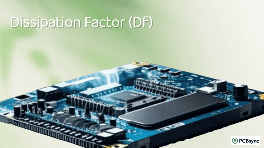
If you’ve spent any time designing high-speed digital circuits or RF boards, you’ve probably come across the term Dissipation Factor (Df)—and if you haven’t paid much attention to it, you might be leaving performance on the table.
I’ve seen engineers obsess over trace widths and impedance matching while completely overlooking Df, only to wonder later why their 10 Gbps signals look like garbage at the receiver. The truth is, as signal speeds keep climbing and frequencies push into the multi-GHz range, Dissipation Factor (Df) has become one of the most critical parameters for PCB material selection.
In this guide, I’ll walk you through everything you need to know about Df—what it actually means, why it matters for your designs, how to select materials based on it, and some practical tips I’ve picked up over the years.
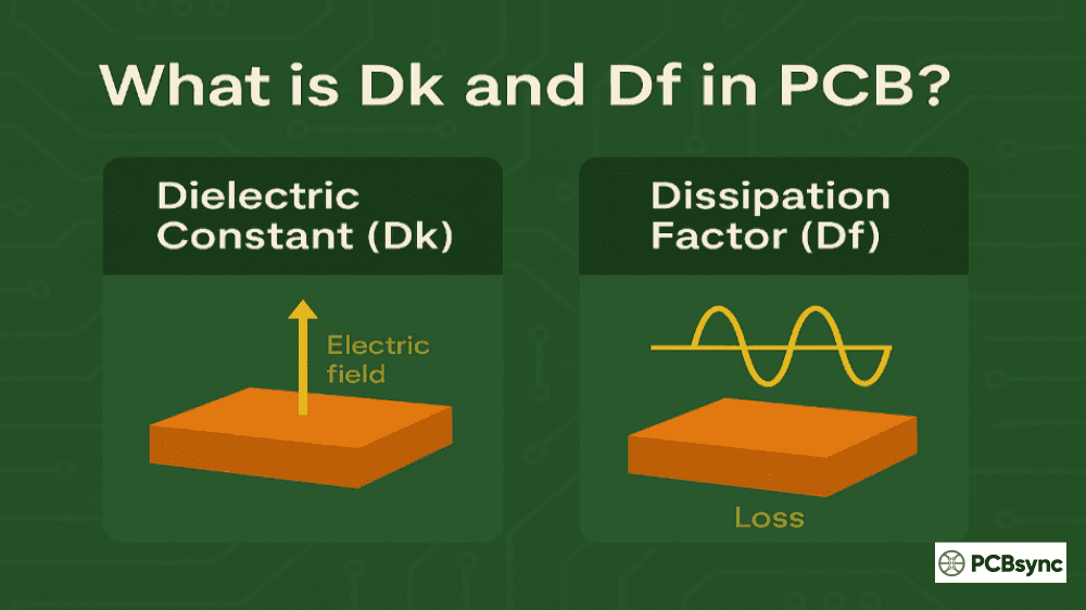
Dissipation Factor (Df), also called loss tangent (tan δ), is a measure of how much electromagnetic energy a dielectric material absorbs and converts to heat as a signal propagates through it. In simpler terms, it tells you how “lossy” your PCB substrate is.
When an AC signal travels down a transmission line on your board, the electric field interacts with the dielectric material between the signal trace and the reference plane. In a perfect world, all that energy would just keep moving down the line. In reality, some of it gets absorbed by the molecular structure of the dielectric and dissipated as heat.
The mathematical definition is straightforward:
Df = tan δ = ε” / ε’
Where:
ε” is the imaginary part of permittivity (representing loss)
ε’ is the real part of permittivity (representing energy storage)
For us PCB designers, what this boils down to is: the lower the Df value, the less signal loss you’ll experience.
How Dissipation Factor (Df) Relates to Signal Loss
The dielectric loss component of total insertion loss can be approximated by:
This formula shows why Df becomes increasingly important at higher frequencies—the loss scales directly with frequency. At 1 GHz, you might not notice the difference between FR4 and a low-loss material. At 10 GHz or 25 Gbps data rates, that difference becomes the determining factor in whether your design works or fails.
Why Dissipation Factor (Df) Matters in Modern PCB Design
The High-Speed Design Challenge
Back when most designs ran at a few hundred MHz, Df was largely an afterthought. Standard FR4 with a Df around 0.02 worked fine for most applications. But consider where we are now:
DDR5 memory runs at data rates exceeding 6400 MT/s
PCIe 5.0 operates at 32 GT/s per lane
100G/400G Ethernet requires channels supporting 25-56 Gbps per lane
5G and mmWave applications push into 28 GHz and beyond
At these speeds, even a few inches of trace can accumulate significant losses. The Nyquist frequency for 25 Gbps signaling is 12.5 GHz—that’s already well into the territory where Df dominates your loss budget.
Impact on Signal Integrity
High Dissipation Factor (Df) causes several signal integrity problems:
1. Amplitude Attenuation Signals arrive at the receiver with reduced voltage swing, eating into your noise margin. For marginal receivers, this can push bit error rates above acceptable thresholds.
2. Rise Time Degradation Higher frequencies experience more attenuation than lower frequencies, effectively filtering your edge transitions. This is why “lossy” materials are sometimes called “low-pass filter” substrates—they round off your signal edges.
3. Inter-Symbol Interference (ISI) When edge rates degrade, adjacent bits start interfering with each other. This ISI is often the killer for high-speed serial links running without equalization.
4. Reduced Timing Margin The combination of amplitude loss and rise time degradation eats into your timing budget, particularly for parallel buses where skew matters.
Understanding Dissipation Factor (Df) Values
Typical Df Ranges for PCB Materials
Not all PCB materials are created equal. Here’s how they generally break down:
PTFE (Teflon): Lowest Df, but more expensive and harder to process
PPE/PPO blends: Good balance of Df and processability
The glass weave reinforcement also plays a role. E-glass has a higher Dk than the resin, creating an inhomogeneous dielectric. This is why some advanced materials use spread glass or alternative glass types to reduce fiber weave effects.
Frequency Dependence
Dissipation Factor (Df) isn’t constant across all frequencies—it generally increases with frequency for most materials. This is why laminate datasheets typically specify Df at multiple frequency points (often 1 GHz, 5 GHz, and 10 GHz).
When comparing materials, make sure you’re looking at Df values measured at the same frequency. A material with Df = 0.005 at 1 GHz might have Df = 0.008 at 10 GHz.
Temperature Effects
Here’s something that doesn’t get enough attention: Df changes with temperature. Research has shown that PCB materials can exhibit 10-35% higher Df values at elevated operating temperatures (50-75°C) compared to room temperature measurements.
This matters because:
Your board isn’t operating at the 23°C room temperature where datasheets are measured
Hot spots near processors and power components see even higher temperatures
Some resin systems are more temperature-stable than others
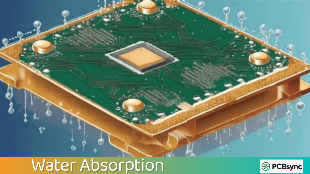
Moisture Absorption
Moisture in the dielectric increases both Dk and Df. Materials with lower moisture absorption (typically specified as a percentage after 24-hour immersion) maintain more stable electrical properties in humid environments.
Resin Content
The ratio of resin to glass affects Df. Higher resin content generally means lower Df since the glass has higher loss than most resin systems. However, this is a tradeoff—higher resin content can affect mechanical properties and CTE.
How to Select PCB Materials Based on Dissipation Factor (Df)
Step 1: Determine Your Frequency/Data Rate Requirements
Start by identifying your highest-frequency signals:
Application Type
Data Rate
Nyquist Freq
Recommended Max Df
USB 2.0
480 Mbps
240 MHz
0.025 (FR4 OK)
PCIe 3.0
8 GT/s
4 GHz
0.015
PCIe 4.0
16 GT/s
8 GHz
0.010
PCIe 5.0
32 GT/s
16 GHz
0.005
25G Ethernet
25 Gbps
12.5 GHz
0.004
56G PAM4
56 Gbps
14 GHz
0.003
Step 2: Calculate Your Loss Budget
Your total insertion loss budget depends on:
Transmitter output amplitude
Receiver sensitivity
Acceptable BER (bit error rate)
Available equalization (Tx pre-emphasis, Rx CTLE/DFE)
A rough rule of thumb for modern high-speed SerDes: try to keep channel loss under 20-25 dB at Nyquist. Beyond that, you’re relying heavily on equalization, which increases power consumption and can impact latency.
Step 3: Consider the Full Stackup
Don’t just focus on the signal layers. For stripline configurations, your signal is sandwiched between two reference planes, so the dielectric properties of adjacent layers matter.
A common cost-optimization approach: use low-loss materials only for layers adjacent to high-speed signals, and use standard FR4 for power planes and non-critical areas. This “hybrid stackup” can significantly reduce material costs.
Step 4: Factor in Manufacturing Considerations
Some materials require special processing:
PTFE materials need different drill parameters and can’t be plated using standard processes
Some low-loss materials have limited availability in certain thicknesses
Hybrid stackups with different materials can introduce registration challenges
Work with your fabricator early to understand their capabilities and material inventory.
Measuring and Testing Dissipation Factor (Df)
Standard Test Methods for Df
Several test methods exist for measuring Dissipation Factor (Df), and they can produce different results:
Test Method
Standard
Frequency Range
Notes
Split Post Cavity Resonator
IPC-TM-650 2.5.5.5
Spot frequencies
Common for datasheets
IPC Stripline
IPC-TM-650 2.5.5.5
1-10 GHz
Good correlation to PCB
Bereskin Stripline
—
1-20 GHz
Wider frequency range
Ring Resonator
—
Multiple resonances
Shows frequency dependence
Full Sheet Resonance
IPC-TM-650 2.5.5.6
Spot frequencies
In-plane measurement
The key takeaway: when comparing materials from different suppliers, make sure they’re using the same test method. A Df value measured using a resonator method might differ from one measured using a stripline method.
In-Circuit Validation
For critical designs, don’t rely solely on datasheet values. Build test vehicles and measure actual insertion loss using a VNA (Vector Network Analyzer). This captures the real-world combination of:
Dielectric loss (from Df)
Conductor loss (from copper roughness)
Radiation and coupling losses
Many PCB fabricators offer impedance and insertion loss testing as a value-added service.
Practical Design Tips for Managing Dissipation Factor (Df)
Tip 1: Route High-Speed Signals on Inner Layers
Stripline configurations (signal between two planes) typically show lower total loss than microstrip (signal on outer layer) because the fields are more contained in the dielectric and less affected by solder mask losses.
Tip 2: Use Low-Profile Copper
Copper surface roughness contributes to conductor loss, which adds to your total insertion loss. For high-speed designs, specify low-profile (LP) or very low-profile (VLP) foils. The smoother copper surface reduces losses at high frequencies.
Tip 3: Minimize Trace Length
This sounds obvious, but it’s worth emphasizing: the best way to reduce loss is shorter traces. Work with your component placement to minimize critical trace lengths. Sometimes moving a connector 2 inches can make the difference between a working design and a failed one.
Tip 4: Consider Reference Plane Stitching
At multi-GHz frequencies, return path discontinuities cause additional loss and reflections. Ensure adequate stitching vias near signal layer transitions and around connectors.
Tip 5: Watch Your Via Stubs
Via stubs create resonances that appear as additional loss at specific frequencies. For high-speed designs, use back-drilling or blind/buried vias to minimize stubs.
The Cost-Performance Tradeoff
Let’s be honest: low-loss materials are expensive. Here’s a rough cost comparison relative to standard FR4:
Material Type
Relative Cost
When to Use
Standard FR4
1×
< 3 GHz, cost-critical
High-Perf FR4
1.5–2×
Up to 10 Gbps, moderate reach
Megtron 4
2–3×
10-25 Gbps applications
Megtron 6
3–4×
25+ Gbps, long traces
Rogers 4350B
5–8×
RF, microwave
PTFE (RT/duroid)
8–12×
mmWave, aerospace
The right approach isn’t always “lowest loss possible”—it’s matching the material to your actual requirements. Using Megtron 6 for a design that could work on enhanced FR4 just wastes money.
Common Mistakes When Dealing with Dissipation Factor (Df)
Mistake 1: Ignoring Df Until Validation I’ve seen teams spec standard FR4, build prototypes, and then be surprised when their 25 Gbps links don’t work. Simulate your channel loss early, including realistic Df values.
Mistake 2: Using Datasheet Df at Wrong Frequency Datasheets often highlight Df at 1 GHz, which looks great. But if your Nyquist is 12 GHz, you need the Df value at that frequency—which could be 2-3× higher.
Mistake 3: Forgetting About Temperature Room temperature Df values don’t tell the whole story. If your board operates in a hot enclosure, factor in the temperature coefficient of Df.
Mistake 4: Treating Hybrid Stackups Carelessly Mixing materials with different Dk values can create impedance discontinuities at layer transitions. Work with your fabricator to ensure proper impedance control.
Mistake 5: Overlooking the Glass Weave At high frequencies, the fiber weave pattern can cause skew in differential pairs. Use spread glass or route at an angle to the weave pattern for critical signals.
Future Trends in Low-Df PCB Materials
The demand for ever-lower Dissipation Factor (Df) materials continues to grow:
Megtron 7 from Panasonic pushes Df down to 0.0015 at 1 GHz
New resin systems combining low loss with improved mechanical properties
Alternative reinforcements beyond traditional E-glass
Liquid crystal polymer (LCP) substrates for mmWave applications
For the next generation of 112 Gbps PAM4 and beyond, material development will be crucial to keeping channel losses manageable.
Useful Resources for PCB Material Selection
Here are some valuable resources for engineers working with Dissipation Factor (Df) and PCB material selection:
Online Material Selectors and Databases
Sierra Circuits Material Selector: Interactive tool comparing 50+ rigid and 10+ flex materials with Dk, Df, Tg, and other properties
Panasonic Electronic Materials – Megtron series documentation
Technical documentation for Megtron 4/6/7
Standards and Test Methods
IPC-4101: Specification for Base Materials for Rigid and Multilayer Printed Boards
IPC-TM-650: Test Methods Manual (includes Dk/Df test procedures)
Design Tools
Altium Designer – Layer Stack Manager with material database
Cadence Allegro – Integrated impedance and loss calculators
Polar Instruments – Si9000 for transmission line modeling
FAQs About Dissipation Factor (Df) in PCB
What is a good Dissipation Factor (Df) for high-speed PCB design?
For most high-speed applications running at 10+ Gbps, you’ll want a Dissipation Factor (Df) of 0.005 or lower at your operating frequency. For 25+ Gbps designs or long traces, aim for Df ≤ 0.003. Standard FR4 with Df around 0.02 is only suitable for applications below 3-5 GHz. The exact requirement depends on your trace length, loss budget, and available equalization.
What is the difference between Dissipation Factor (Df) and Loss Tangent?
They’re the same thing—just different names. Dissipation Factor (Df) and Loss Tangent (tan δ) both describe the ratio of energy lost to energy stored in a dielectric material. PCB manufacturers tend to use “Dissipation Factor” while academic and physics literature often uses “Loss Tangent.” When you see tan δ in a formula, you can substitute Df directly.
How does Dissipation Factor (Df) change with frequency?
Dissipation Factor (Df) generally increases with frequency for most PCB materials. A material might have Df = 0.004 at 1 GHz but Df = 0.006 at 10 GHz. This frequency dependence varies by material—some advanced materials maintain more stable Df across frequency. Always check the Df value at the frequency relevant to your design, not just the headline number at 1 GHz.
Can I use standard FR4 for RF applications?
Standard FR4 is generally not recommended for RF applications above a few GHz due to its high Dissipation Factor (Df) of 0.018-0.025. The high Df causes excessive signal loss, and FR4’s dielectric constant varies significantly with frequency, causing unpredictable impedance. For RF circuits, materials like Rogers RO4350B (Df = 0.0037) or RO4003C (Df = 0.0027) are much better choices despite the higher cost.
How do I reduce the effects of high Dissipation Factor (Df) in my design?
If you’re stuck with higher-Df materials due to cost constraints, you can mitigate the impact by: (1) minimizing trace lengths for critical high-speed signals, (2) routing on stripline layers rather than microstrip to reduce radiation loss, (3) using low-profile copper foils to reduce conductor loss, (4) implementing equalization at the receiver, and (5) increasing transmitter drive strength if possible. However, there’s no substitute for proper material selection—these are workarounds, not solutions.
Conclusion
Dissipation Factor (Df) has evolved from a secondary specification to a primary design driver as signal speeds continue to increase. Understanding Df and its impact on signal integrity is essential for any engineer working on high-speed digital, RF, or mixed-signal designs.
The key takeaways:
Df directly determines dielectric loss, which scales with frequency
Lower Df = less signal loss, but also higher cost
Match your material to your actual requirements—don’t over-specify or under-specify
Consider the full picture: temperature, moisture, frequency dependence, and manufacturing constraints
Whether you’re designing a server backplane running 56 Gbps PAM4 or an automotive radar module at 77 GHz, getting Dissipation Factor (Df) right is fundamental to a successful design. Take the time early in your project to analyze your loss budget and select appropriate materials—it’s much easier than trying to fix signal integrity problems after your boards are built.
Inquire: Call 0086-755-23203480, or reach out via the form below/your sales contact to discuss our design, manufacturing, and assembly capabilities.
Quote: Email your PCB files to Sales@pcbsync.com (Preferred for large files) or submit online. We will contact you promptly. Please ensure your email is correct.
Notes: For PCB fabrication, we require PCB design file in Gerber RS-274X format (most preferred), *.PCB/DDB (Protel, inform your program version) format or *.BRD (Eagle) format. For PCB assembly, we require PCB design file in above mentioned format, drilling file and BOM. Click to download BOM template To avoid file missing, please include all files into one folder and compress it into .zip or .rar format.


