Inquire: Call 0086-755-23203480, or reach out via the form below/your sales contact to discuss our design, manufacturing, and assembly capabilities.
Quote: Email your PCB files to Sales@pcbsync.com (Preferred for large files) or submit online. We will contact you promptly. Please ensure your email is correct.
Notes: For PCB fabrication, we require PCB design file in Gerber RS-274X format (most preferred), *.PCB/DDB (Protel, inform your program version) format or *.BRD (Eagle) format. For PCB assembly, we require PCB design file in above mentioned format, drilling file and BOM. Click to download BOM template To avoid file missing, please include all files into one folder and compress it into .zip or .rar format.
If you’ve spent any time designing high-speed or RF circuits, you’ve probably wrestled with the dielectric constant (Dk) of your PCB substrate. It’s one of those specifications that seems straightforward on paper but can cause serious headaches when your impedance calculations don’t match reality. After years of working with various laminate materials, I’ve learned that understanding Dk isn’t just about memorizing numbers from a datasheet—it’s about knowing how this property actually behaves in your specific design conditions.
The dielectric constant, also known as relative permittivity (εr), measures how much a material can store electrical energy compared to a vacuum. For PCB engineers, it directly impacts trace impedance, signal propagation speed, and overall circuit performance. A vacuum has a Dk of exactly 1.0, while common PCB materials range from about 2.2 to 10+, depending on the composition.
Understanding the Fundamentals of Dielectric Constant (Dk)
When we talk about the dielectric constant in PCB materials, we’re essentially describing how the substrate affects the electric field between conductors. Think of it this way: if you have a parallel-plate capacitor filled with air, it stores a certain amount of charge at a given voltage. Replace that air with FR4, and the same capacitor stores about 4.5 times more charge. That ratio is the dielectric constant.
The mathematical relationship is relatively simple. The Dk value equals the permittivity of the material divided by the permittivity of free space (ε₀ = 8.854 × 10⁻¹² F/m). What makes things complicated in practice is that this “constant” isn’t constant at all—it varies with frequency, temperature, moisture content, and even the material thickness.
Why Dk Values on Datasheets Can Be Misleading
Here’s something that took me years to fully appreciate: the Dk values published on material datasheets are measured under specific conditions that may not match your application. Most manufacturers test at 1 MHz using IPC-TM-650 test methods, but your high-speed digital design might operate at 5 GHz or higher. The difference can be significant.
For instance, standard FR4 might show a dielectric constant of 4.7 at 1 MHz, but at 1 GHz, it drops to around 4.2, and at 10 GHz, it might be closer to 4.15. Rogers Corporation recognized this issue and introduced “Design Dk” values—these are measured using the differential phase length method at frequencies more relevant to actual circuit operation. If your laminate supplier doesn’t provide frequency-dependent Dk data, consider that a red flag.
How Dielectric Constant Affects Your PCB Design
The dielectric constant influences almost every aspect of high-frequency PCB design. Let me break down the critical areas where you’ll feel its impact.
Signal Propagation Speed and Dk Relationship
The velocity at which signals travel through your transmission lines is inversely proportional to the square root of the Dk. In a vacuum, signals travel at the speed of light (approximately 3 × 10⁸ m/s). On a PCB with FR4 (Dk ≈ 4.4), that speed drops to roughly half—about 1.43 × 10⁸ m/s. This directly affects timing calculations, especially in designs where signal arrival times need to be matched across different trace lengths.
The formula is straightforward: V = C / √Dk, where V is the propagation velocity, C is the speed of light, and Dk is the dielectric constant. For high-speed digital designs running at multiple Gbps, even small Dk variations can throw off your timing budget.
Controlled Impedance and Trace Width Calculations
This is where the dielectric constant really shows its importance. The characteristic impedance of a microstrip or stripline depends heavily on Dk. A higher Dk means you need narrower traces to achieve the same impedance target. For a 50Ω microstrip on FR4 with a 10-mil dielectric thickness, you might need a trace width around 18 mils. Switch to a Rogers material with Dk of 3.0, and that same 50Ω impedance requires a wider trace—perhaps 28 mils.
The practical implication? If the Dk value in your design software doesn’t match the actual material Dk, your fabricated board won’t hit your impedance targets. I’ve seen boards come back with 45Ω traces when 50Ω was specified, all because the designer used a generic Dk value instead of the correct one for their specific laminate thickness and copper weight.
Factors That Influence Dielectric Constant in PCB Materials
Understanding what affects the dielectric constant helps you anticipate problems before they become expensive failures. Here are the key factors every PCB engineer should consider:
Frequency Dependence: Most PCB materials exhibit decreasing Dk as frequency increases. This is due to the inability of molecular dipoles to keep up with rapidly oscillating electric fields. FR4 might drop from 4.7 at 1 MHz to 4.15 at 10 GHz—a 12% reduction that significantly affects your impedance calculations at high frequencies.
Temperature Effects: The thermal coefficient of dielectric constant (TCDk) describes how Dk changes with temperature. A material with high TCDk will cause impedance drift as your board heats up during operation. For temperature-critical applications, look for materials with TCDk below ±50 ppm/°C.
Moisture Absorption: Water has a Dk of approximately 70—dramatically higher than any PCB material. When your board absorbs moisture, even a small percentage can significantly increase the effective Dk. This is why low moisture absorption rates (below 0.1%) are critical for outdoor or humid environment applications.
Glass-to-Resin Ratio: In composite materials like FR4, the Dk varies based on the proportion of glass reinforcement to epoxy resin. Glass has a higher Dk (around 6.1 for E-glass) than epoxy resin (around 3.2). Thinner laminates often have different glass-to-resin ratios, which is why Dk can vary with material thickness.
Material Anisotropy: The Dk isn’t the same in all directions. Most PCB materials are anisotropic—the Dk measured in the Z-direction (through the board thickness) differs from the X-Y plane. Manufacturers typically specify Z-direction Dk since that’s what affects stripline and microstrip performance, but anisotropy matters for certain embedded component designs.
Comparing Dielectric Constant Values Across Common PCB Materials
Choosing the right material requires understanding the trade-offs between different Dk values, cost, and performance. The following table summarizes typical values for commonly used PCB laminates:
Note: Dk and Df values vary by manufacturer specifications, laminate thickness, and test frequency. Always consult the specific manufacturer datasheet for your chosen thickness and copper weight configuration.
How to Measure and Verify Dielectric Constant
Getting accurate Dk measurements is critical for precision designs. The PCB industry uses several standardized methods, each with its own strengths and limitations.
IPC-TM-650 Standard Test Methods for Dk
The IPC has developed multiple test methods for measuring dielectric constant, each suited to different frequency ranges and material types:
Test Method
Frequency Range
Description
IPC-TM-650 2.5.5.3
1 MHz
Two-fluid cell method for thin films and laminates
IPC-TM-650 2.5.5.5
8 – 12.4 GHz
Clamped stripline resonator (X-band)
IPC-TM-650 2.5.5.6
0.25 – 2.2 GHz
Full sheet resonance (FSR) non-destructive test
IPC-TM-650 2.5.5.15
1 – 20 GHz
Split-post dielectric resonator (SPDR)
One critical insight from industry studies: different test methods can yield significantly different Dk values for the same material. A 2010 IPC study found that laminate supplier datasheets and higher-frequency test methods often showed substantial variation. This is why trusting a single Dk number from a datasheet can be problematic for precision applications.
Practical Dk Verification Using TDR
For engineers who want to verify dielectric constant on actual fabricated boards, Time Domain Reflectometry (TDR) provides a practical approach. The method relies on measuring propagation delay along a known-length transmission line and back-calculating the effective Dk.
The basic relationship is: Dk = (c × td / L)², where c is the speed of light, td is the propagation delay, and L is the physical trace length. While this gives you an effective Dk that includes fringing field effects (for microstrip), it represents what your signals actually experience—which is often more useful than a raw material Dk from a datasheet.
Selecting the Right Dielectric Constant for Your Application
Choosing the optimal Dk value involves balancing performance requirements against cost and manufacturability. Here’s a framework I use when advising on material selection:
Application Type
Recommended Dk Range
Key Considerations
Consumer electronics (<1 GHz)
4.0 – 4.8 (FR4)
Cost-sensitive; standard FR4 adequate
High-speed digital (1-10 Gbps)
3.4 – 4.0
Low-loss Df critical; stable Dk over frequency
Very high-speed (25+ Gbps)
3.0 – 3.6
Ultra-low loss; Dk stability critical
RF/Microwave (2-20 GHz)
2.2 – 3.5
Low Dk for larger features; tight Dk tolerance
mmWave (>30 GHz)
2.2 – 3.0
PTFE-based; minimal Dk variation with frequency
Using Hybrid Stackups to Optimize Dk and Cost
One strategy I frequently recommend is using hybrid stackups that combine different dielectric constant materials within the same board. The concept is straightforward: use premium low-Dk, low-loss materials only where you need them (high-speed signal layers), and use standard FR4 for power distribution and less critical routing layers.
For example, a 12-layer design might use Megtron 6 for the top and bottom signal layers where 25 Gbps SerDes signals run, but standard high-Tg FR4 for the inner power planes and lower-speed I/O routing. This approach can cut material costs by 40-50% compared to an all-premium stackup while maintaining signal integrity where it matters.
The catch is manufacturability. Different materials have different coefficients of thermal expansion (CTE), and mixing them can create reliability issues if not done carefully. Always work with your fabricator early to validate any hybrid stackup approach.
Practical Design Tips for Managing Dielectric Constant
After working on hundreds of high-speed designs, I’ve developed a set of practical guidelines for working with Dk values effectively:
Always use frequency-appropriate Dk values: If your signals have significant frequency content at 5 GHz, don’t use the 1 MHz Dk from the datasheet. Request the Design Dk or measure it yourself using TDR on test coupons.
Account for thickness variation: The dielectric constant varies with laminate thickness because of different glass-to-resin ratios. A 4-mil core will have a different Dk than a 10-mil core of the same material family. Use Dk values specific to your chosen thickness.
Include Dk tolerance in your impedance budget: If a material specifies Dk = 3.5 ± 0.05, that ±1.4% variation translates to about ±0.7% impedance variation. Add this to your overall impedance tolerance stack.
Specify copper roughness: Rough copper increases effective Dk by creating a transition region between conductor and dielectric. For precision RF work, specify smooth or reverse-treat copper foils.
Use field solvers, not formulas: Closed-form impedance formulas work well for initial estimates, but for production designs, always verify with a 2D field solver that properly models the actual stackup geometry and material properties.
Frequently Asked Questions About Dielectric Constant (Dk)
What is a good dielectric constant for high-speed PCB design?
For high-speed digital designs running above 10 Gbps, a Dk value between 3.0 and 4.0 is typically ideal. Lower Dk allows faster signal propagation and larger trace widths, but the dissipation factor (Df) is equally important—look for Df below 0.005 for best signal integrity. Materials like Isola FR408HR (Dk ≈ 3.65) or Megtron 6 (Dk ≈ 3.4) are common choices for designs in the 25+ Gbps range.
Why does dielectric constant change with frequency?
The dielectric constant decreases with increasing frequency due to polarization effects in the material. At low frequencies, molecular dipoles in the resin and glass can fully align with the oscillating electric field, contributing to higher polarization and higher Dk. As frequency increases, these dipoles can’t keep up with rapid field changes, reducing their contribution. This is called dielectric dispersion, and it’s most pronounced in composite materials like FR4.
How does dielectric constant affect trace impedance?
The characteristic impedance of a transmission line is inversely related to the square root of the Dk. A higher Dk means lower impedance for the same trace geometry, so you need narrower traces to achieve the same target impedance. For example, to achieve 50Ω on FR4 (Dk ≈ 4.4), you might need an 18-mil trace width, while the same 50Ω on Rogers RO4003C (Dk ≈ 3.38) requires about 22 mils at equivalent dielectric thickness.
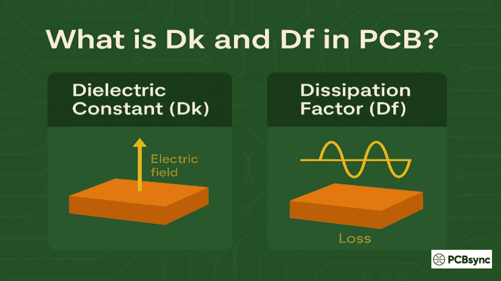
What is the difference between Dk and Df in PCB materials?
The dielectric constant (Dk) measures how much the material slows down signals and affects impedance. The dissipation factor (Df), also called loss tangent, measures how much signal energy is converted to heat as it passes through the material. While Dk affects impedance and propagation delay, Df directly impacts signal attenuation. For high-frequency applications, both must be low—Dk for proper impedance control and Df for minimal signal loss.
Is Rogers material always better than FR4 for high-frequency designs?
Not always. Rogers materials excel in RF and microwave applications where their low Dk, ultra-low loss, and tight Dk tolerance are essential. However, they cost 5-15× more than FR4 and can be harder to manufacture. For applications below 3-5 GHz where modest signal loss is acceptable, high-performance FR4 variants (like Isola 370HR or FR408HR) often provide sufficient performance at much lower cost. The right choice depends on your specific frequency, loss budget, and cost constraints.
Conclusion: Making Dk Work for Your Design
Understanding dielectric constant (Dk) is fundamental to successful high-frequency PCB design. The key takeaways from this guide are: always use frequency-appropriate Dk values rather than the 1 MHz numbers on datasheets; account for material thickness effects on Dk; include Dk tolerance in your impedance budget; and work with your fabricator early to validate material selections and stackup designs.
The dielectric constant isn’t just a number to plug into your impedance calculator—it’s a property that varies with frequency, temperature, and material composition. By understanding these variations and designing accordingly, you’ll avoid the costly surprises that come from treating Dk as truly “constant.” Remember, what matters most is the effective Dk your signals actually experience in operation, not the idealized values from a specification sheet.
Whether you’re designing consumer electronics on standard FR4 or pushing the limits with 112 Gbps PAM-4 signaling on ultra-low-loss laminates, the principles remain the same: understand your material, validate your assumptions, and design with appropriate margins for real-world variation.
Inquire: Call 0086-755-23203480, or reach out via the form below/your sales contact to discuss our design, manufacturing, and assembly capabilities.
Quote: Email your PCB files to Sales@pcbsync.com (Preferred for large files) or submit online. We will contact you promptly. Please ensure your email is correct.
Notes: For PCB fabrication, we require PCB design file in Gerber RS-274X format (most preferred), *.PCB/DDB (Protel, inform your program version) format or *.BRD (Eagle) format. For PCB assembly, we require PCB design file in above mentioned format, drilling file and BOM. Click to download BOM template To avoid file missing, please include all files into one folder and compress it into .zip or .rar format.


