Inquire: Call 0086-755-23203480, or reach out via the form below/your sales contact to discuss our design, manufacturing, and assembly capabilities.
Quote: Email your PCB files to Sales@pcbsync.com (Preferred for large files) or submit online. We will contact you promptly. Please ensure your email is correct.
Notes: For PCB fabrication, we require PCB design file in Gerber RS-274X format (most preferred), *.PCB/DDB (Protel, inform your program version) format or *.BRD (Eagle) format. For PCB assembly, we require PCB design file in above mentioned format, drilling file and BOM. Click to download BOM template To avoid file missing, please include all files into one folder and compress it into .zip or .rar format.
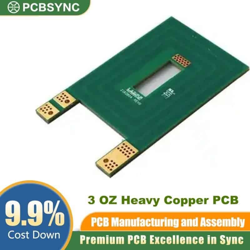
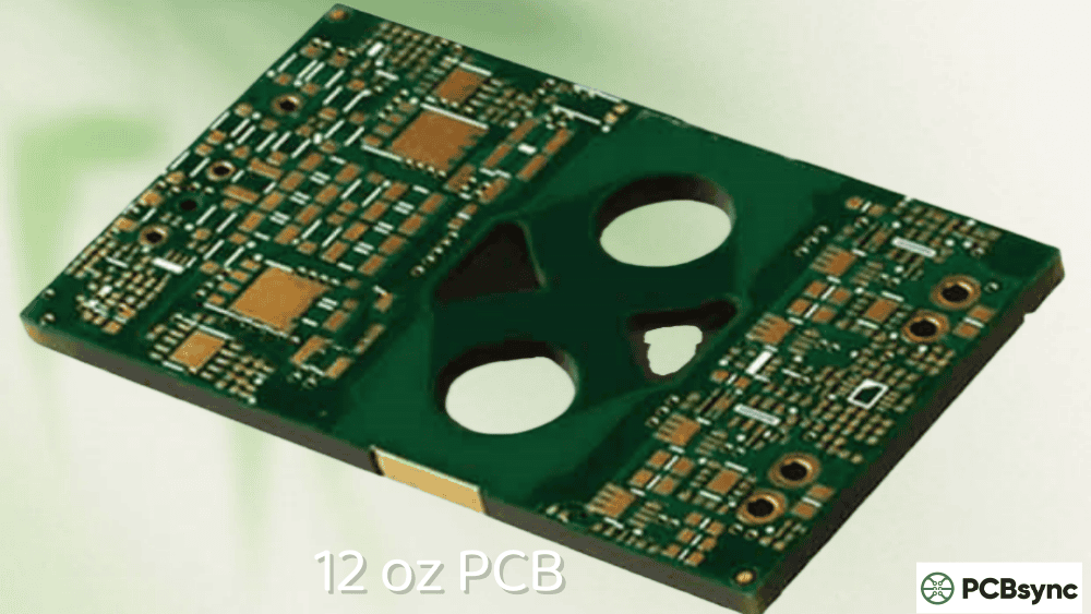
If you’re designing high-power electronics and standard circuit boards just aren’t cutting it, you’ve probably landed on 12 oz PCB as a potential solution. I’ve worked with heavy copper boards for over a decade in power supply and EV applications, and I can tell you: understanding when and how to use 12 oz copper makes the difference between a reliable product and one that fails in the field.
This guide covers everything you need to know about 12 oz PCB design, manufacturing, and applications. No fluff—just practical information you can actually use.
A 12 oz PCB is a heavy copper printed circuit board with a copper thickness of 12 ounces per square foot. In practical terms, that translates to 420 μm (0.42mm) or approximately 16.44 mils of copper thickness.
To put that in perspective, most standard PCBs use 1 oz copper (35 μm). A 12 oz board has twelve times that amount of copper, which dramatically changes what the board can do.
Here’s the thing most guides don’t tell you: copper weight directly determines your current-carrying capacity and thermal performance. More copper means lower resistance, better heat dissipation, and the ability to handle currents that would fry a standard board.
12 oz Copper Thickness Conversion Chart
Copper Weight
Thickness (μm)
Thickness (mils)
Thickness (mm)
1 oz
35
1.37
0.035
2 oz
70
2.76
0.070
4 oz
140
5.51
0.140
6 oz
210
8.27
0.210
8 oz
280
11.02
0.280
10 oz
350
13.78
0.350
12 oz
420
16.44
0.420
14 oz
490
19.29
0.490
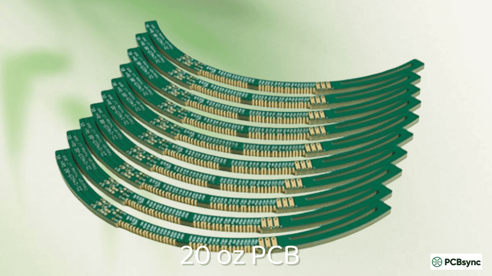
20 oz
700
27.56
0.700
Why Choose 12 oz PCB Over Standard Copper?
I’ve seen engineers default to adding more layers instead of increasing copper weight. That’s often the wrong approach for high-power applications. Here’s why 12 oz copper makes sense:
Superior Current Handling Capacity
The cross-sectional area of your trace determines how much current it can carry. A 12 oz copper trace has 12 times the cross-sectional area of a 1 oz trace at the same width. This means you can either carry more current with the same trace width, or achieve the same current capacity with narrower traces.
Real-world example: A 100-mil wide trace on a 12 oz PCB can safely carry over 50A with acceptable temperature rise. The same trace on a 1 oz board? Maybe 4-5A.
Excellent Thermal Management
Copper has a thermal conductivity of approximately 385-401 W/m·K. That thick copper layer acts as a built-in heat spreader, pulling heat away from components and distributing it across the board surface. I’ve measured 15-20°C temperature reductions in power converter designs simply by upgrading from 4 oz to 12 oz copper.
Mechanical Durability
Thicker copper provides structural reinforcement. This matters in applications with vibration, thermal cycling, or mechanical stress. The plated-through holes (PTHs) are particularly robust with heavy copper—they can handle thousands of thermal cycles without barrel cracking.
Getting your design right the first time saves money and headaches. These are the rules I follow:
Minimum Trace Width and Spacing Requirements
Heavy copper etching is different from standard PCB processing. The thicker the copper, the more undercutting occurs during etching. This means you need wider traces and larger gaps than you might expect.
Based on IPC-2221 guidelines with 10°C temperature rise above ambient:
Trace Width (mil)
Trace Width (mm)
External Layer Current
Internal Layer Current
25
0.64
~15A
~10A
50
1.27
~25A
~17A
100
2.54
~45A
~30A
150
3.81
~60A
~42A
200
5.08
~75A
~52A
250
6.35
~90A
~62A
Note: These are approximations. Always verify with IPC-2152 calculations or thermal simulation for critical applications.
Stackup Considerations
When designing multilayer boards with 12 oz copper, balance your stackup. If you have 12 oz on layers 1 and 4, consider matching copper weight on opposing layers to prevent warping during thermal cycles.
A common approach I use:
Outer layers: 12 oz (power distribution)
Inner layers: 2-4 oz (signal routing and additional power planes)
The prepreg selection matters too. You need sufficient resin to fill the gaps created by thick copper traces. Work with your fabricator early—they’ll know what prepreg combinations work for your stackup.
Manufacturing 12 oz copper boards isn’t just “more of the same” compared to standard PCBs. The process requires specialized techniques:
Copper Plating Methods
Two main approaches exist:
Standard Etching (for up to 10 oz): Start with heavy copper-clad laminate and etch away unwanted copper. The challenge is achieving clean trace edges—ordinary etching produces excessive undercut at these thicknesses.
Step Plating/Differential Etching (for 10+ oz): This is the preferred method for 12 oz PCB. The manufacturer builds up copper thickness through multiple plating cycles, then uses differential etching to create the final traces. This produces straighter sidewalls and tighter tolerances.
Solder Mask Challenges
Standard screen-printed solder mask doesn’t work well on heavy copper. The ink pools in the valleys beside tall traces, leaving thin coverage on trace tops. Quality manufacturers use electrostatic spraying instead, which deposits uniform solder mask thickness regardless of copper topography.
Drilling and PTH Plating
The plated-through holes need extra attention. With 12 oz copper, the aspect ratio of holes changes significantly. Manufacturers typically use:
Carbide or diamond-coated drill bits
Multiple drilling passes
Extended copper plating times to build adequate barrel thickness
Via Design for Heavy Copper
Via design becomes critical with 12 oz copper. Thermal vias connected to copper planes help transfer heat from hot components to the board surface. For effective thermal management, consider:
Via diameter: Larger holes (0.4-0.6mm) allow better copper plating coverage and lower thermal resistance.
Via density: Place 5+ thermal vias per square centimeter under high-power components.
Via filling: Copper-filled vias provide the best thermal and electrical performance but add cost. Conductive epoxy fill offers a middle-ground solution.
Via-in-pad: Acceptable with heavy copper if properly filled and capped. Essential for BGA packages on power components.
Beyond the basics, here are advantages that often get overlooked:
Reduced EMI and Noise
The broad copper surfaces in 12 oz PCB enable effective low-pass filtering. High-speed communication systems that struggle with electromagnetic interference benefit from the reduced ground bounce and improved shielding that thick copper provides.
Environmental Resistance
12 oz copper boards using CEM (Composite Epoxy Material) substrates show excellent resistance to moisture, temperature extremes, and chemical exposure. The glass transition temperature (Tg) of properly specified boards exceeds 280°C, ensuring stability under demanding conditions.
Extended Product Lifespan
The combination of thermal stability and mechanical strength means 12 oz PCB designs typically outlast equivalent standard copper implementations by factors of 3-5x in accelerated life testing. For products with 10+ year service requirements, this reliability advantage justifies the higher initial cost.
Simplified Assembly
Interestingly, despite the design complexity, 12 oz boards can simplify assembly. The thick copper acts as a heat sink during soldering, requiring higher temperatures and longer dwell times, but it also eliminates the need for external heat sinks in many applications. Fewer separate components means fewer potential failure points.
Applications for 12 oz Heavy Copper PCB
Where does 12 oz PCB actually make sense? These are the applications where I’ve seen it succeed:
Electric Vehicle (EV) Power Systems
EVs are driving massive demand for heavy copper boards. Battery management systems (BMS), motor controllers, onboard chargers, and DC-DC converters all benefit from 12 oz copper. A typical EV motor controller might handle 200-400A—that requires serious copper.
Industrial Power Supplies
Switch-mode power supplies (SMPS), especially those above 500W, often use heavy copper. The power stage carries high currents at low voltages, making trace resistance a significant factor in efficiency.
Solar Inverters and Energy Storage
Grid-tie inverters and battery storage systems need to convert and manage substantial power. A 10kW solar inverter handles peak currents that would overwhelm standard PCBs. Heavy copper ensures reliability over a 25-year system lifespan.
Railway and Transportation Electronics
Railway traction systems, signaling equipment, and auxiliary power supplies face extreme vibration and temperature swings. The mechanical robustness of 12 oz copper helps these boards survive where lighter copper would fail.
Aerospace and Defense
Radar systems, weapon controls, and avionics require maximum reliability in harsh environments. Heavy copper’s ability to handle thermal stress and maintain electrical performance makes it standard for military-grade electronics.
12 oz PCB vs 10 oz PCB: Which Should You Choose?
This is a question I get frequently. The honest answer: it depends on your margins.
Parameter
10 oz PCB
12 oz PCB
Copper Thickness
350 μm (13.78 mil)
420 μm (16.44 mil)
Current Capacity
~20% less than 12 oz
Baseline
Thermal Performance
Good
Better
Min Trace/Space
18-20 mil
20-25 mil
Manufacturing Cost
Lower
~15-25% higher
Availability
More common
Fewer qualified suppliers
If you’re right at the edge of 10 oz capability, go with 12 oz. The extra cost is negligible compared to field failures. If you have comfortable margin with 10 oz, save the money.
Cost Factors for 12 oz PCB Production
Heavy copper costs more. Here’s what drives the price:
Material Cost: Copper-clad laminate for 12 oz costs significantly more than standard 1 oz material. Copper prices fluctuate, so quotes can vary.
Processing Time: Multiple plating cycles, extended etching times, and additional inspection steps all add labor cost.
Yield Rate: Heavy copper boards have higher scrap rates. Manufacturers build this into their pricing.
Minimum Order: Not all fabricators stock 12 oz material. You might face higher minimums or setup charges.
Budget estimate: Expect to pay 3-5x the cost of an equivalent standard copper board for prototype quantities. Volume pricing improves this ratio.
Common Mistakes to Avoid
From years of reviewing designs, these are the errors I see most often:
Ignoring Etching Compensation: Your fabricator needs to compensate trace widths for etch undercut. Provide your target dimensions and let them adjust the artwork. Don’t guess at compensation values yourself.
Insufficient Annular Ring: Heavy copper needs larger pads around vias and holes. Plan for minimum 10 mil annular ring, preferably 15 mil.
Asymmetric Stackup: Unbalanced copper distribution causes warping. Mirror your copper weights around the board center.
Skipping Thermal Simulation: At 12 oz, the board itself becomes part of your thermal solution. Model the heat flow, don’t just assume the copper will handle it.
Not Involving the Fabricator Early: Heavy copper is specialized. Get your manufacturer’s design rules before you start layout, not after you’ve submitted Gerbers.
Useful Resources and Tools
Here are the resources I keep bookmarked:
Design Calculators
Saturn PCB Toolkit – Free Windows application with trace width, via current, and thermal calculations
What is the maximum current a 12 oz PCB can handle?
There’s no single answer—it depends on trace width, acceptable temperature rise, and whether the trace is on an internal or external layer. A 200-mil wide external trace on 12 oz copper can handle approximately 75A with 10°C rise. For precise values, use IPC-2152 calculations with your specific parameters.
Can 12 oz copper be used in multilayer PCBs?
Yes, but with limitations. Most fabricators can produce multilayer boards with 12 oz copper on outer layers and up to 10-12 oz on inner layers. The key constraints are overall board thickness, prepreg selection, and lamination pressure. Discuss your requirements with potential suppliers before finalizing your stackup.
How does 12 oz PCB cost compare to standard PCB?
Expect to pay 3-5x more for 12 oz copper boards compared to equivalent 1 oz designs in prototype quantities. Volume production narrows this gap somewhat. The cost premium comes from material expense, longer processing times, and lower manufacturing yields.
What surface finishes work with 12 oz heavy copper?
All standard finishes work: HASL (lead-free), ENIG, immersion silver, OSP, and immersion tin. ENIG is often recommended for heavy copper because it provides a flat surface that helps compensate for the topography created by thick copper traces. Discuss with your manufacturer which finish they recommend for your specific application.
How do I find a reliable 12 oz PCB manufacturer?
Look for fabricators who specifically list heavy copper capabilities (10+ oz) in their published specifications. Ask for references from similar projects. Request sample boards before committing to production. Key questions: What’s their experience with your target copper weight? What are their actual (not theoretical) tolerances? Can they provide test reports showing copper thickness measurements?
Final Thoughts
12 oz PCB isn’t for every project, but when you need it, nothing else will do. The combination of current capacity, thermal performance, and mechanical durability makes it essential for serious high-power applications.
The key is understanding the design rules, working with qualified manufacturers, and not treating heavy copper like standard PCB. Plan for the differences in trace width, spacing, and stackup from the start of your design.
If you’re moving from standard copper to 12 oz for the first time, start with a prototype run. Verify your thermal assumptions, check your manufacturing partner’s capabilities, and build in margin. The boards cost more, but they’ll deliver the performance your high-power application demands.
Have questions about 12 oz PCB design for your specific application? Drop them in the comments below.
Inquire: Call 0086-755-23203480, or reach out via the form below/your sales contact to discuss our design, manufacturing, and assembly capabilities.
Quote: Email your PCB files to Sales@pcbsync.com (Preferred for large files) or submit online. We will contact you promptly. Please ensure your email is correct.
Notes: For PCB fabrication, we require PCB design file in Gerber RS-274X format (most preferred), *.PCB/DDB (Protel, inform your program version) format or *.BRD (Eagle) format. For PCB assembly, we require PCB design file in above mentioned format, drilling file and BOM. Click to download BOM template To avoid file missing, please include all files into one folder and compress it into .zip or .rar format.


