Inquire: Call 0086-755-23203480, or reach out via the form below/your sales contact to discuss our design, manufacturing, and assembly capabilities.
Quote: Email your PCB files to Sales@pcbsync.com (Preferred for large files) or submit online. We will contact you promptly. Please ensure your email is correct.
Notes: For PCB fabrication, we require PCB design file in Gerber RS-274X format (most preferred), *.PCB/DDB (Protel, inform your program version) format or *.BRD (Eagle) format. For PCB assembly, we require PCB design file in above mentioned format, drilling file and BOM. Click to download BOM template To avoid file missing, please include all files into one folder and compress it into .zip or .rar format.
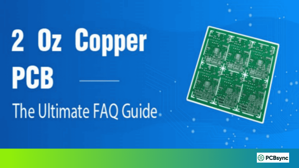
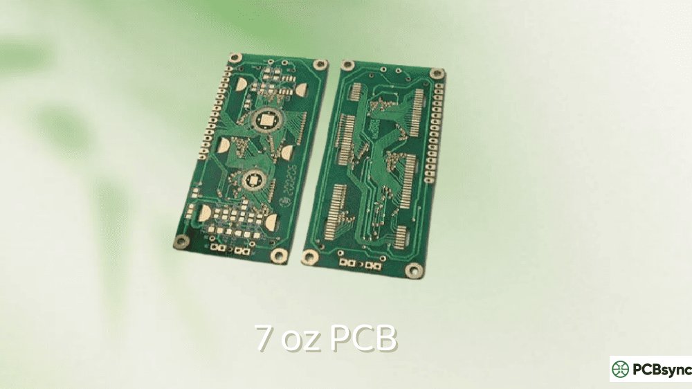
When you’re designing power electronics and the standard 1-2 oz copper just won’t cut it, but jumping straight to extreme heavy copper feels like overkill, there’s a sweet spot that many engineers overlook. 7 oz PCB technology sits right in that critical middle ground, offering substantial current-carrying capacity without the manufacturing complexity of ultra-heavy copper boards.
After spending fifteen years in PCB design and fabrication, I’ve seen countless projects where 7 oz copper was exactly what the application needed. This guide breaks down everything you need to know about 7 oz PCB technology, from design considerations to real-world applications.
A 7 oz PCB refers to a printed circuit board with copper foil weighing 7 ounces per square foot. To put this in perspective, standard consumer electronics typically use 1 oz copper (approximately 35 μm thick). At 7 oz, we’re talking about copper thickness of roughly 245 μm or 9.6 mils, which is seven times the standard thickness.
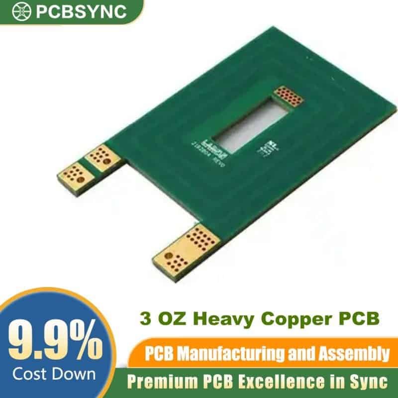
This copper weight classification places 7 oz PCB firmly in the heavy copper category, which generally starts at 3 oz and extends beyond 20 oz for extreme applications. The “in-between” nature of 7 oz copper makes it particularly versatile for applications that demand more than moderate heavy copper but don’t require the extreme thermal mass of 10+ oz designs.
Understanding Copper Weight Measurements
The copper weight system might seem counterintuitive at first. We measure copper thickness by how much a square foot of the foil would weigh. Here’s how 7 oz PCB compares across the spectrum:
Copper Weight
Thickness (μm)
Thickness (mils)
Category
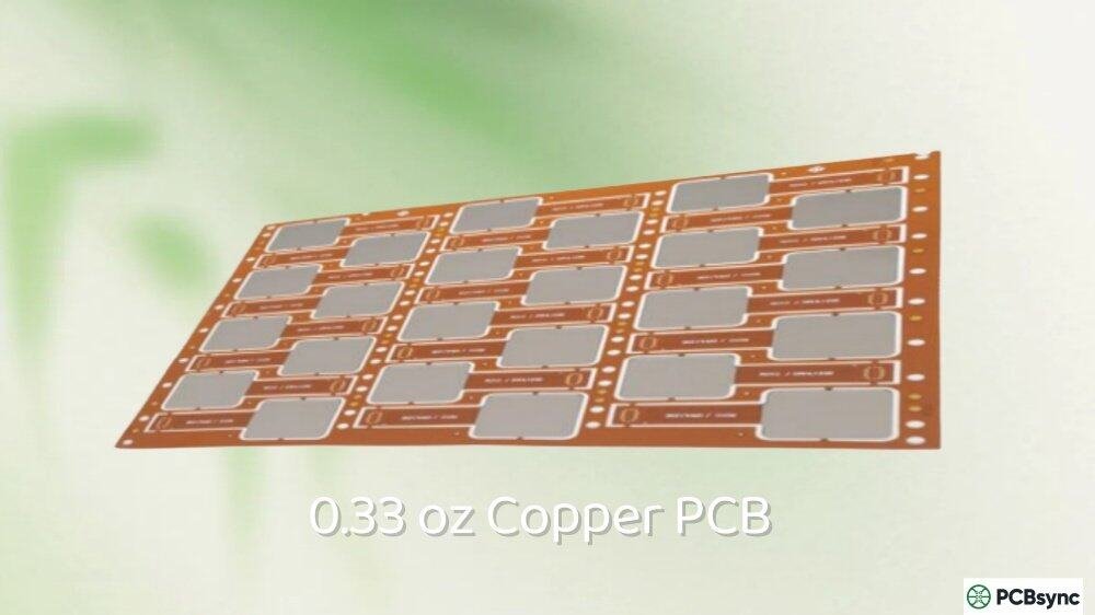
0.5 oz
17.5
0.7
Standard
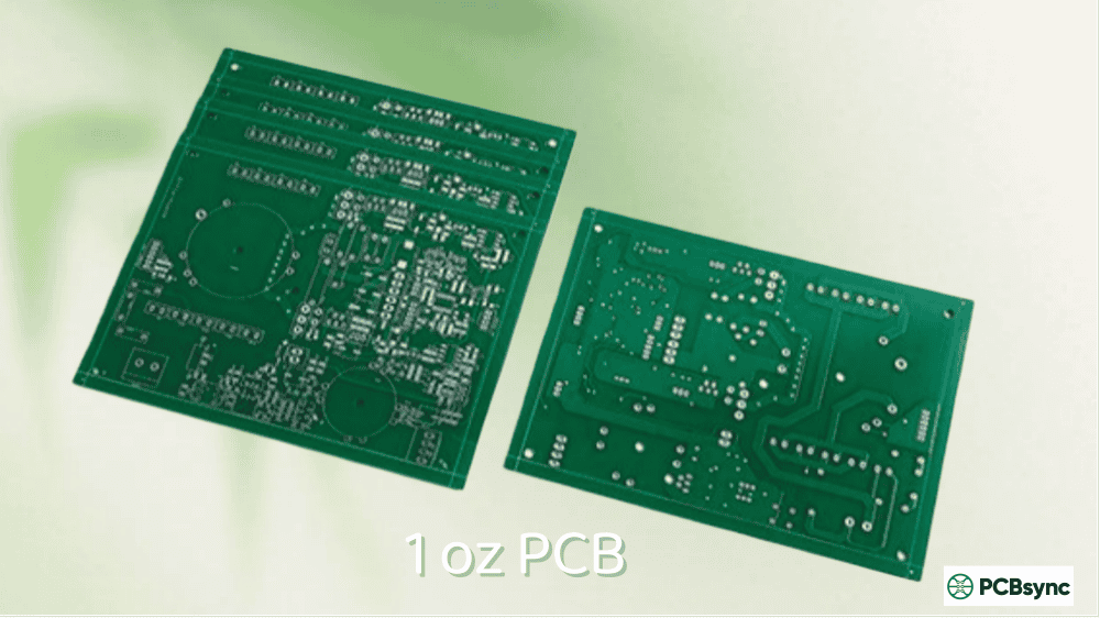
1 oz
35
1.4
Standard
2 oz
70
2.8
Standard
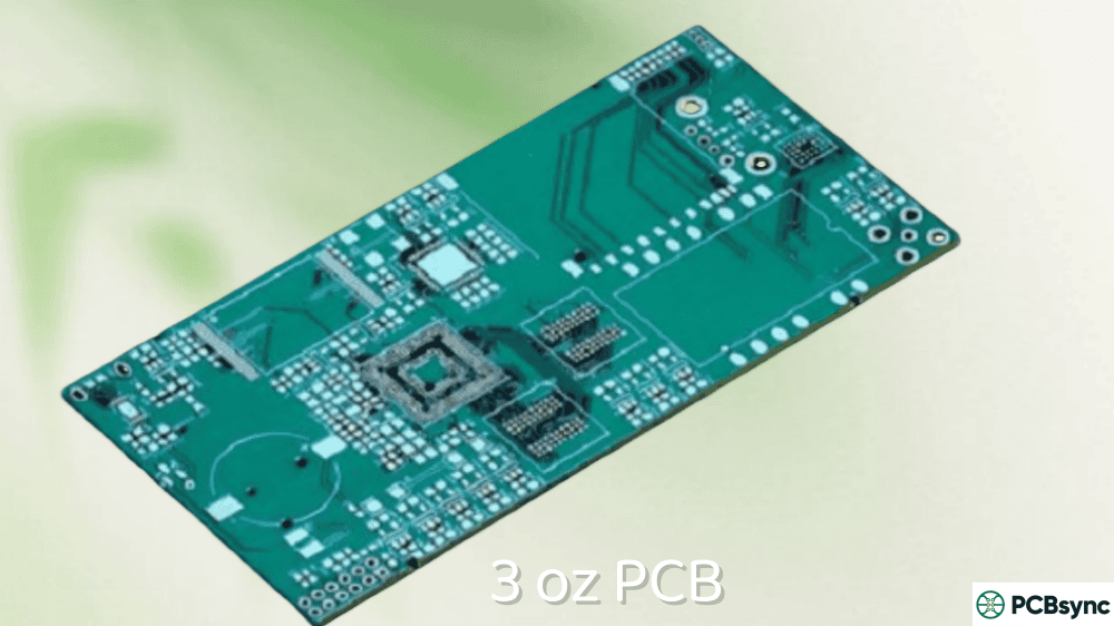
3 oz
105
4.1
Heavy Copper
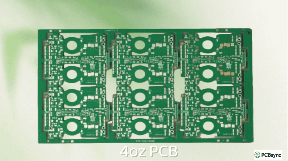
4 oz
140
5.5
Heavy Copper
7 oz
245
9.6
Heavy Copper
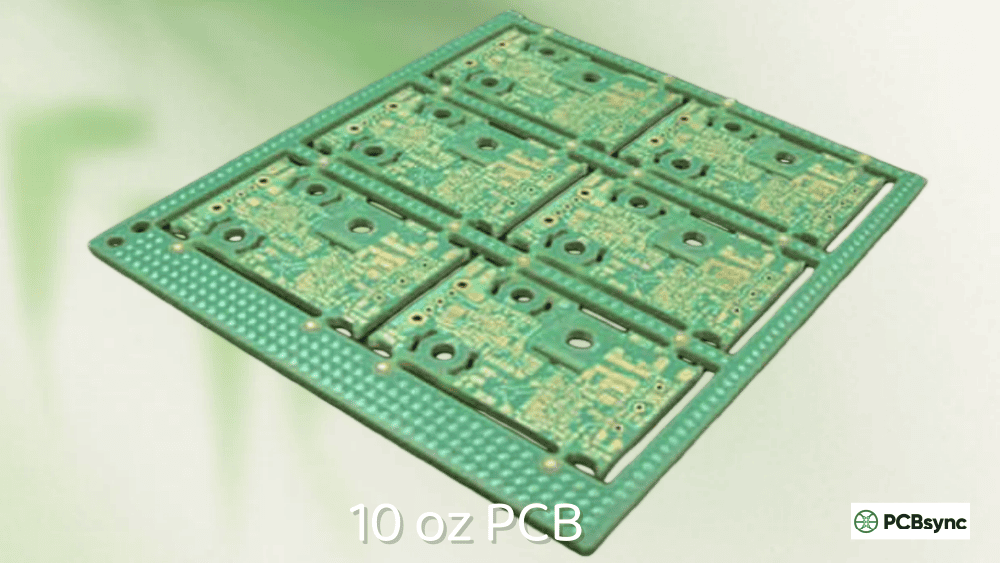
10 oz
350
13.8
Extreme Heavy
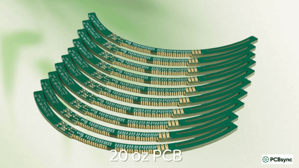
20 oz
700
27.6
Extreme Heavy
Why Choose 7 oz PCB for Your Design?
When I consult with design teams on copper weight selection, the conversation always starts with current requirements and thermal management needs. Here’s why 7 oz PCB often emerges as the optimal choice:
Superior Current Carrying Capacity
The relationship between copper thickness and current capacity isn’t linear, but thicker copper dramatically increases ampacity. A 7 oz trace can handle approximately 3-4 times the current of a 2 oz trace at equivalent widths. For power conversion circuits running 30-50A continuous, 7 oz copper allows reasonable trace widths without consuming excessive board real estate.
Enhanced Thermal Performance
Heat dissipation becomes critical in power electronics, and 7 oz PCB excels here. The thermal conductivity of copper (approximately 385 W/m·K) combined with the substantial cross-sectional area means heat spreads efficiently across the board surface. I’ve seen operating temperatures drop by 15-25°C simply by upgrading from 3 oz to 7 oz copper in high-power designs.
Mechanical Robustness
Thicker copper adds structural rigidity to the PCB assembly. In applications subject to vibration, thermal cycling, or mechanical stress, 7 oz PCB provides significantly better durability than lighter copper weights. The plated through-holes also benefit from the thicker barrel plating, improving connection reliability.
The Balance Factor
This is where 7 oz PCB really shines. You get substantial performance improvements over 4-5 oz copper without the manufacturing challenges that come with 10+ oz designs. Etching precision, layer registration, and overall yield rates remain manageable at 7 oz, keeping costs reasonable while delivering heavy-duty performance.
Based on projects I’ve worked on and industry trends, these applications consistently benefit from 7 oz copper:
Power Electronics and Converters
DC-DC converters, inverters, and power supplies in the 1-10 kW range frequently use 7 oz PCB construction. The copper weight handles the high currents while maintaining thermal stability during continuous operation.
Electric Vehicle Components
EV charging infrastructure, motor controllers, and battery management systems increasingly specify 7 oz PCB for their power stages. The automotive industry’s reliability requirements align well with the robust construction.
Industrial Motor Drives
Variable frequency drives and servo controllers benefit from 7 oz copper in their power sections. These applications often see sustained high-current operation in demanding environments.
Renewable Energy Systems
Solar inverters and wind turbine controllers use 7 oz PCB technology extensively. The boards must handle significant power throughput while surviving outdoor environmental conditions.
High-Power LED Lighting
Commercial and industrial LED fixtures with substantial wattage leverage 7 oz copper for both current handling and thermal management, extending LED lifetime through better heat dissipation.
Application
Typical Current Range
Why 7 oz Works
DC-DC Converters
20-80A
Balanced current/thermal needs
EV Chargers
30-100A
Reliability requirements
Motor Drives
25-60A
Sustained operation cycles
Solar Inverters
15-50A
Environmental durability
LED Drivers
5-30A
Thermal management critical
Design Guidelines for 7 oz PCB
Getting the most from 7 oz copper requires adjusting your design approach. Here are the key considerations I emphasize with design teams:
Trace Width and Spacing Requirements
Heavy copper etching isn’t as precise as standard copper. The thicker the copper, the more undercut occurs during the etching process. For 7 oz PCB, plan for minimum trace widths of 10-12 mils (0.25-0.30 mm) and spacing of at least 12 mils between traces. Some fabricators can achieve tighter tolerances, but these numbers provide safe design margins.
Via and Hole Considerations
Through-hole plating in 7 oz PCB presents unique challenges. The aspect ratio of vias becomes critical, and I recommend minimum via diameters of 0.4mm for reliable plating. Thermal vias connecting to internal planes should be sized generously, typically 0.5-0.6mm, to ensure good thermal transfer.
Layer Stackup Planning
Most 7 oz PCB designs use the heavy copper on outer layers only, with standard weight copper for internal signal layers. This hybrid approach provides the heavy copper benefits where needed while maintaining signal integrity and manufacturing feasibility. Work closely with your fabricator on stackup planning.
Thermal Relief Connections
When connecting heavy copper traces to planes, thermal reliefs become essential for soldering. Without proper thermal reliefs, the massive copper heat sink makes achieving proper solder joints nearly impossible. Design reliefs with 4-6 spokes and adequate clearance.
Design for Manufacturing (DFM)
Engage your PCB fabricator early in the design process. 7 oz PCB manufacturing requires specialized processes, and each shop has specific capabilities. Getting DFM feedback before finalizing your layout saves significant time and money.
Understanding how 7 oz PCB boards are manufactured helps you design more manufacturable products. The process differs from standard PCB fabrication in several key areas:
Copper Deposition Methods
There are two primary approaches to achieving 7 oz copper:
Starting with heavy foil: The laminate begins with 7 oz copper foil bonded to the substrate. This method produces uniform copper thickness but requires specialized materials.
Plating up from lighter copper: Starting with 2-3 oz base copper, additional copper is electroplated to reach the target thickness. This approach allows for mixed copper weights on the same layer but adds process complexity.
Most fabricators use a combination, starting with heavier base foil and plating to final thickness. This balances material costs with process control.
Etching Challenges
Removing 245 μm of copper during pattern definition requires extended etching times and careful process control. The etch factor (ratio of vertical to horizontal etching) becomes critical. Expect some sidewall angle on your traces rather than perfectly vertical walls.
Registration and Alignment
Layer-to-layer registration becomes more challenging with heavy copper due to material movement during processing. Design with adequate registration tolerances and verify capabilities with your chosen fabricator.
Cost Factors for 7 oz PCB Projects
Let’s talk money because budget constraints are real. 7 oz PCB costs more than standard boards, but understanding the cost drivers helps optimize your design:
Cost Factor
Impact Level
Notes
Raw Copper Material
High
7x more copper than standard
Extended Processing Time
Medium-High
Longer etching, plating cycles
Specialized Equipment
Medium
Not all shops equipped
Lower Yield Rates
Medium
More complex processing
Testing Requirements
Low-Medium
Standard electrical test applies
Typical pricing runs 2-4x standard PCB costs, depending on complexity. However, when you factor in the alternative of using bus bars, mechanical heat sinks, or multiple parallel boards, 7 oz PCB often proves cost-effective for the integrated solution it provides.
Quality Standards and Specifications
When specifying 7 oz PCB for your project, reference these industry standards:
IPC-6012: Qualification and Performance Specification for Rigid Printed Boards covers general PCB requirements including heavy copper variants.
IPC-2152: Standard for Determining Current Carrying Capacity in Printed Board Design provides current capacity guidelines for various copper weights.
IPC-A-600: Acceptability of Printed Boards defines inspection criteria applicable to heavy copper construction.
Request Class 2 or Class 3 inspection depending on your application criticality. For automotive or aerospace applications, additional specifications like IATF 16949 or AS9100 compliance may apply.
Useful Resources for 7 oz PCB Design
Here are resources I regularly reference and recommend to engineers working with heavy copper:
What is the maximum current a 7 oz PCB trace can carry?
Current capacity depends on trace width, allowable temperature rise, and ambient conditions. As a rough guideline, a 200 mil (5mm) wide 7 oz trace can carry approximately 35-45A with a 20°C temperature rise above ambient. Always verify with IPC-2152 calculations or thermal simulation for your specific design conditions.
Can 7 oz copper be used on internal layers?
Technically yes, but it’s uncommon and adds significant manufacturing complexity. The increased thickness affects overall board thickness, drilling, and layer registration. Most designs use heavy copper only on outer layers, with standard copper for internal signal routing. Discuss with your fabricator if internal heavy copper is truly necessary.
What surface finishes work with 7 oz PCB?
All standard surface finishes are compatible with 7 oz PCB including HASL, ENIG, OSP, and immersion tin/silver. For high-current connections, HASL often provides good results due to the additional tin thickness. ENIG works well when flat surfaces are critical for component mounting.
How does 7 oz copper affect impedance-controlled designs?
The thicker copper requires adjusted trace geometry calculations for controlled impedance traces. Impedance is still achievable, but trace widths will differ from standard copper designs. Use a stackup calculator that accounts for actual copper thickness, and work with your fabricator to verify achievable tolerances.
What’s the typical lead time for 7 oz PCB fabrication?
Lead times typically run 15-25 business days for prototype quantities, compared to 5-10 days for standard boards. The extended processing times and often limited production slots for heavy copper drive longer lead times. Quick-turn options exist at premium pricing but expect minimum 10 days even for expedited service.
Making the Decision: Is 7 oz PCB Right for Your Project?
After all this technical detail, how do you decide? I use a simple framework with my clients:
Choose 7 oz PCB when your design requires 20-60A continuous current in a compact form factor, needs integrated thermal management without external heat sinks, must survive demanding environmental conditions, and benefits from reduced assembly complexity versus bus bar alternatives.
Consider alternatives when currents exceed 80-100A (look at bus bars or extreme heavy copper), thermal requirements can be met with IMS substrates, budget constraints are severe and standard copper with derating can work, or lead time is critical and standard boards suffice.
The 7 oz PCB occupies a valuable middle ground in the heavy copper spectrum. It’s capable enough for serious power applications yet manufacturable without exotic processes. For the right application, it’s often the optimal choice that balances performance, cost, and practicality.
When you’re ready to move forward with a 7 oz PCB design, start conversations with potential fabricators early. Their specific capabilities and design guidelines will shape your final layout, and the collaboration typically results in better outcomes for everyone involved.
Inquire: Call 0086-755-23203480, or reach out via the form below/your sales contact to discuss our design, manufacturing, and assembly capabilities.
Quote: Email your PCB files to Sales@pcbsync.com (Preferred for large files) or submit online. We will contact you promptly. Please ensure your email is correct.
Notes: For PCB fabrication, we require PCB design file in Gerber RS-274X format (most preferred), *.PCB/DDB (Protel, inform your program version) format or *.BRD (Eagle) format. For PCB assembly, we require PCB design file in above mentioned format, drilling file and BOM. Click to download BOM template To avoid file missing, please include all files into one folder and compress it into .zip or .rar format.


