Inquire: Call 0086-755-23203480, or reach out via the form below/your sales contact to discuss our design, manufacturing, and assembly capabilities.
Quote: Email your PCB files to Sales@pcbsync.com (Preferred for large files) or submit online. We will contact you promptly. Please ensure your email is correct.
Notes: For PCB fabrication, we require PCB design file in Gerber RS-274X format (most preferred), *.PCB/DDB (Protel, inform your program version) format or *.BRD (Eagle) format. For PCB assembly, we require PCB design file in above mentioned format, drilling file and BOM. Click to download BOM template To avoid file missing, please include all files into one folder and compress it into .zip or .rar format.
I’ve been working with heavy copper boards for over a decade now, and I can tell you that understanding when and how to use 4 oz copper can make or break your high-power design. This guide covers everything from basic specifications to real-world design considerations that textbooks often skip over.
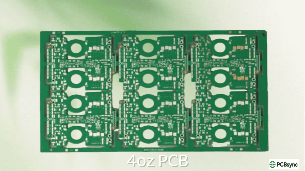
What is 4 oz PCB? Understanding Copper Weight Fundamentals
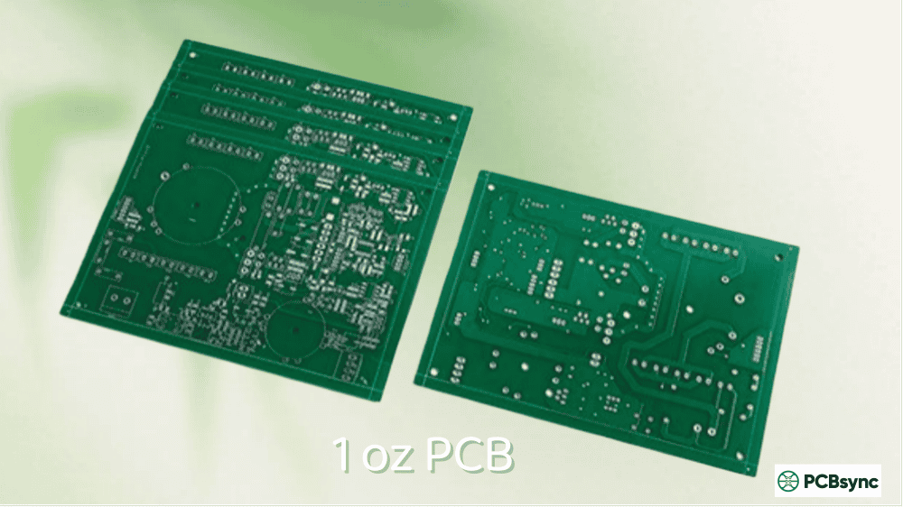
In PCB manufacturing, copper thickness is measured in ounces per square foot (oz/ft²). This measurement tells you how much copper would cover one square foot of board surface. A 4 oz PCB has approximately 140 microns (0.14mm or 5.6 mils) of copper on each conductive layer—that’s four times thicker than the standard 1 oz copper found in most consumer electronics.
Here’s something many engineers don’t realize at first: the “ounce” measurement isn’t about the weight of your finished board. It’s a standardized way to specify copper foil thickness that dates back to early PCB manufacturing. When suppliers talk about “4 oz copper,” they mean a foil that weighs 4 ounces when spread over a one-square-foot area.
The decision to use 4 oz copper PCB usually comes down to three factors: current handling, thermal management, and long-term reliability. Let me break down each one based on what I’ve seen in actual production environments.
Superior Current Carrying Capacity
The most obvious advantage of 4 oz copper is its ability to handle significantly higher currents. According to IPC-2152 standards, a 4 oz copper trace can carry roughly 3-4 times the current of a 1 oz trace at the same width and temperature rise. For a 10mm wide trace with a 10°C temperature rise above ambient, you’re looking at approximately 70 amps capacity with 4 oz copper versus around 17 amps with 1 oz.
This isn’t just theoretical. On a motor controller project I worked on last year, we needed to route 40A continuous through a relatively compact board. With 1 oz copper, we would have needed traces over 25mm wide—completely impractical for the form factor. Switching to 4 oz copper let us achieve the same current with traces under 8mm wide.
Table 2: Current Capacity Comparison (10°C Rise, External Layer)
Trace Width
1 oz Copper
2 oz Copper
4 oz Copper
5mm
~8A
~14A
~35A
10mm
~17A
~30A
~70A
15mm
~25A
~45A
~100A
20mm
~32A
~58A
~130A
Note: Values are approximate. Always verify with IPC-2152 calculator for your specific conditions.
Enhanced Thermal Management for 4 oz PCB
Heat dissipation is where 4 oz copper really shines, and it’s often underappreciated. Copper has a thermal conductivity of about 400 W/m·K—roughly 1000 times better than FR-4 substrate material. When you increase copper thickness from 1 oz to 4 oz, you’re essentially adding a much more effective heat spreader directly onto your board.
In practical terms, this means hot spots around power components spread heat more evenly across the board surface. I’ve measured temperature reductions of 15-25°C on MOSFET packages just by switching from 2 oz to 4 oz copper on the power plane, without any other design changes. That’s the difference between needing an external heatsink and not needing one.
Improved Mechanical Strength and Reliability
Thicker copper provides better mechanical support for connectors, mounting holes, and plated through-holes. This becomes critical in applications subject to vibration or thermal cycling. The thicker copper walls in vias and PTHs are much more resistant to cracking from thermal expansion stress.
Industry data shows that boards with 2.5 mil (approximately 4 oz equivalent after plating) copper in PTH walls have near-zero failure rates in thermal cycling tests, compared to significant failure rates with standard plating thicknesses.
4 oz PCB Applications: Where Heavy Copper Makes Sense
Not every project needs 4 oz copper PCB. The extra cost and manufacturing complexity only make sense for specific applications. Here’s where I consistently see 4 oz boards delivering real value.
Automotive Electronics and Electric Vehicles
The automotive sector—especially electric vehicles—has become one of the biggest drivers of 4 oz PCB demand. Battery Management Systems (BMS) need to safely route substantial battery currents while minimizing voltage drops. A typical EV battery pack might require handling 100-400A during charging or acceleration.
Battery Management Systems (BMS) for EVs and hybrid vehicles
DC/DC converters and onboard chargers
Motor controllers and inverters
Power Distribution Units (PDUs)
Charging station infrastructure
Industrial Power Electronics and Control Systems
Industrial applications often combine high power with demanding environmental conditions. Motor drives for conveyor systems, CNC machines, and robotics regularly handle 20-50A continuous current in elevated ambient temperatures. The thermal margin provided by 4 oz copper becomes essential for reliable operation.
Variable frequency drives (VFDs) and servo drives
Welding equipment power supplies
Industrial control panels
High-power LED driver circuits
Solar inverters and charge controllers
Aerospace and Defense Systems
Aerospace applications push PCBs to their physical limits with extreme temperature ranges, vibration, and reliability requirements. Systems must perform flawlessly across temperature swings from -55°C to +125°C while handling high continuous currents.
Avionics power control systems
Radar system power supplies
Satellite power distribution
Military vehicle electronics
Table 3: 4 oz PCB Application Summary
Industry Sector
Typical Current Range
Key Requirements
Automotive/EV
50-400A
Thermal cycling, reliability
Industrial
20-100A
Continuous operation, heat
Aerospace
10-80A
Extreme temps, vibration
Renewable Energy
30-150A
Long-term reliability, heat
Telecom/5G
15-50A
High frequency, thermal
4 oz PCB Design Guide: Best Practices for Engineers
Designing with 4 oz copper isn’t just about dropping thicker copper into your existing layout. The manufacturing process differences and thermal considerations require specific design adaptations. Here’s what I’ve learned works in production.
Trace Width and Spacing Requirements for 4 oz PCB
Thicker copper requires wider spacing between traces and larger minimum trace widths. This is because the etching process takes longer for thick copper, and the etchant eats away at the copper sidewalls (undercutting) while it’s working down through the thickness. Most fabricators compensate by slightly increasing your trace widths, but you need to design with adequate spacing from the start.
Table 4: Minimum Trace/Space Requirements by Copper Weight
Copper Weight
Min Trace (mils)
Min Space (mils)
Notes
1 oz
4-5
4-5
Standard capability
2 oz
6-8
6-8
Common heavy copper
3 oz
8-10
10-12
Extended capability
4 oz
10-12
12-16
Verify with fab house
6 oz
14-16
18-20
Specialty fabricators
Important: These are general guidelines. Always confirm minimum feature sizes with your specific PCB manufacturer.
Layer Stackup Considerations for Heavy Copper Boards
A well-designed stackup is crucial for 4 oz PCB success. The general approach I recommend is using 4 oz copper on the layers that carry high current (typically outer layers for power distribution) while keeping inner signal layers at 1-2 oz copper. This provides a good balance between current capacity and routing density.
For a typical 4-layer power board, consider: Layer 1 (Top) – 4 oz copper for power traces; Layer 2 – 1 oz copper for ground plane; Layer 3 – 1 oz copper for signals; Layer 4 (Bottom) – 4 oz copper for power return. This balanced approach prevents warping issues that can occur when copper distribution is uneven.
Even with 4 oz copper’s excellent thermal conductivity, proper thermal design is essential. Here are the key strategies I use:
Thermal vias under hot components: Use arrays of vias (0.3-0.5mm diameter, spaced at 1-1.5mm) under power components like MOSFETs and IGBTs to transfer heat to inner planes or the opposite side of the board.
Copper pours on all layers: Fill unused board area with copper connected to ground or power planes. This provides additional thermal mass and heat spreading capability.
Consider thermal relief patterns: While direct connections provide better thermal and electrical performance, thermal reliefs may be needed for large copper areas to enable proper soldering.
Metal core substrates for extreme cases: When 4 oz copper alone isn’t enough, consider aluminum or copper core PCBs combined with heavy copper for maximum heat dissipation.
Via Design for High-Current 4 oz PCB Applications
Standard vias can become a bottleneck in high-current designs. The typical 1 oz copper plating in via walls may not handle the current density or thermal stress of heavy copper applications. For 4 oz PCB designs, I recommend:
Minimum via diameter of 0.3mm (12 mils) for current-carrying vias
Request 2 oz minimum copper plating in via walls
Use multiple vias in parallel for high-current paths (calculate 2-3A per standard via)
Consider filled and capped vias for components with thermal pads
Material Selection for 4 oz Copper PCB
Standard FR-4 works fine for many 4 oz applications, but for high-temperature environments, consider high-Tg (glass transition temperature) materials. Standard FR-4 has a Tg around 130-140°C, while high-Tg materials reach 170-180°C. For the most demanding applications, polyimide substrates can handle continuous operation at 250°C.
Table 5: Substrate Material Comparison for 4 oz PCB
Material
Tg (°C)
Max Operating
Best For
Standard FR-4
130-140
105°C
General applications
High-Tg FR-4
170-180
140°C
Automotive, industrial
Polyimide
250+
200°C
Aerospace, high-temp
Metal Core (Al)
N/A
150°C+
LED, power modules
Surface Finish Options for 4 oz Copper PCB
The surface finish affects both solderability and long-term reliability. For 4 oz copper PCB applications, the most common choices are:
HASL (Hot Air Solder Leveling): Cost-effective and provides excellent solderability. Lead-free HASL is available for RoHS compliance. Works well for most power electronics.
ENIG (Electroless Nickel Immersion Gold): Provides a flat surface ideal for fine-pitch components and excellent corrosion resistance. Higher cost but better for mixed-technology boards.
OSP (Organic Solderability Preservative): Lowest cost option with good solderability, but limited shelf life. Best for high-volume production with quick turnover.
4 oz PCB Manufacturing: What Engineers Need to Know
Manufacturing 4 oz copper PCB is more complex than standard boards, and not every fabricator can do it well. Understanding the manufacturing challenges helps you set realistic expectations and choose the right supplier.
Common Manufacturing Challenges with Heavy Copper
The longer etching times required for 4 oz copper create several challenges. Undercutting (where etchant eats away copper under the mask) becomes more pronounced, potentially causing trace width variations. Lamination must be carefully controlled to prevent inner layer misregistration. Via plating needs special attention to ensure void-free fill and consistent wall thickness.
Lead times are typically 1.5-2x longer than standard boards. For prototypes, expect 2-3 weeks minimum; production runs may take 4-6 weeks depending on complexity. Plan your schedule accordingly.
How to Choose a 4 oz PCB Manufacturer
When evaluating fabricators for 4 oz PCB work, look for:
Documented experience with heavy copper boards (ask for case studies)
ISO 9001 certification and UL approval for the copper weights you need
AOI (Automated Optical Inspection) and X-ray inspection capabilities
Willingness to provide DFM feedback before production
On-time delivery rate above 95%
Useful Resources and Design Tools for 4 oz PCB
Here are the resources I use regularly when designing heavy copper boards:
Sierra Circuits IPC-2152 Calculator: protoexpress.com/tools/trace-width-and-current-capacity-calculator/
Altium IPC-2221 Calculator: Built into Altium Designer PCB Editor
Saturn PCB Toolkit: Free download with comprehensive PCB calculations
Industry Standards for Heavy Copper PCB Design
IPC-2152: Standard for Determining Current Carrying Capacity in PCBs (replaces IPC-2221 for current calculations)
IPC-2221: Generic Standard on Printed Board Design (general PCB design guidelines)
IPC-6012: Qualification and Performance Specification for Rigid PCBs
IPC-4101: Specification for Base Materials for Rigid and Multilayer PCBs
Frequently Asked Questions About 4 oz PCB
1. What is the actual thickness of 4 oz copper PCB?
A 4 oz copper PCB has copper layers approximately 140 microns (0.14mm or 5.6 mils) thick. This is based on the weight of copper that would cover one square foot of board surface—4 ounces spread evenly over that area equals roughly 140 µm thickness. Remember that this is per layer; a board with 4 oz copper on both outer layers would have 280 µm total copper thickness plus the substrate.
2. How much current can a 4 oz copper PCB handle?
Current capacity depends on trace width, temperature rise, and whether the trace is on an internal or external layer. As a rough guide, a 10mm wide external trace on 4 oz copper can handle approximately 70A with a 10°C temperature rise. For accurate calculations, use IPC-2152 standards and always add safety margin for production variations and worst-case operating conditions.
3. Is 4 oz copper PCB more expensive than standard boards?
Yes, expect to pay 1.5-3x more than equivalent 1 oz boards. The higher cost comes from increased raw material cost, longer processing times (especially etching), tighter process control requirements, and lower yields. However, the cost difference becomes less significant in production volumes, and the improved reliability often reduces total ownership cost for high-power applications.
4. Can I mix different copper weights on the same PCB?
Absolutely, and it’s often the most cost-effective approach. Many designs use 4 oz copper on outer layers for power distribution while keeping inner signal layers at 1-2 oz. Some advanced processes even allow different copper weights on the same layer (embedded copper technology), though this adds complexity and cost.
5. What are the minimum trace width and spacing for 4 oz copper?
Most manufacturers specify minimum trace width of 10-12 mils (0.25-0.3mm) and minimum spacing of 12-16 mils (0.3-0.4mm) for 4 oz copper. These requirements are larger than standard 1 oz boards (typically 4-5 mils) because the longer etching process causes more undercutting. Always verify specific capabilities with your chosen fabricator, as these limits vary.
Final Thoughts on 4 oz PCB Design
4 oz copper PCB technology has become essential for modern power electronics, electric vehicles, and industrial systems. The ability to handle higher currents, dissipate heat more effectively, and provide improved mechanical reliability makes heavy copper boards the right choice for demanding applications.
The key to success is understanding when 4 oz copper is actually needed and designing specifically for its characteristics. Don’t just drop thick copper into a layout designed for 1 oz boards—adjust your trace widths, spacing, via designs, and material selections accordingly. Work with experienced fabricators who understand heavy copper manufacturing, and always get DFM feedback before committing to production.
As power density continues to increase across industries, from EVs to 5G infrastructure to renewable energy systems, 4 oz PCB technology will only become more important. Master these design principles now, and you’ll be well-prepared for the high-power challenges ahead.
Inquire: Call 0086-755-23203480, or reach out via the form below/your sales contact to discuss our design, manufacturing, and assembly capabilities.
Quote: Email your PCB files to Sales@pcbsync.com (Preferred for large files) or submit online. We will contact you promptly. Please ensure your email is correct.
Notes: For PCB fabrication, we require PCB design file in Gerber RS-274X format (most preferred), *.PCB/DDB (Protel, inform your program version) format or *.BRD (Eagle) format. For PCB assembly, we require PCB design file in above mentioned format, drilling file and BOM. Click to download BOM template To avoid file missing, please include all files into one folder and compress it into .zip or .rar format.


