Inquire: Call 0086-755-23203480, or reach out via the form below/your sales contact to discuss our design, manufacturing, and assembly capabilities.
Quote: Email your PCB files to Sales@pcbsync.com (Preferred for large files) or submit online. We will contact you promptly. Please ensure your email is correct.
Notes: For PCB fabrication, we require PCB design file in Gerber RS-274X format (most preferred), *.PCB/DDB (Protel, inform your program version) format or *.BRD (Eagle) format. For PCB assembly, we require PCB design file in above mentioned format, drilling file and BOM. Click to download BOM template To avoid file missing, please include all files into one folder and compress it into .zip or .rar format.
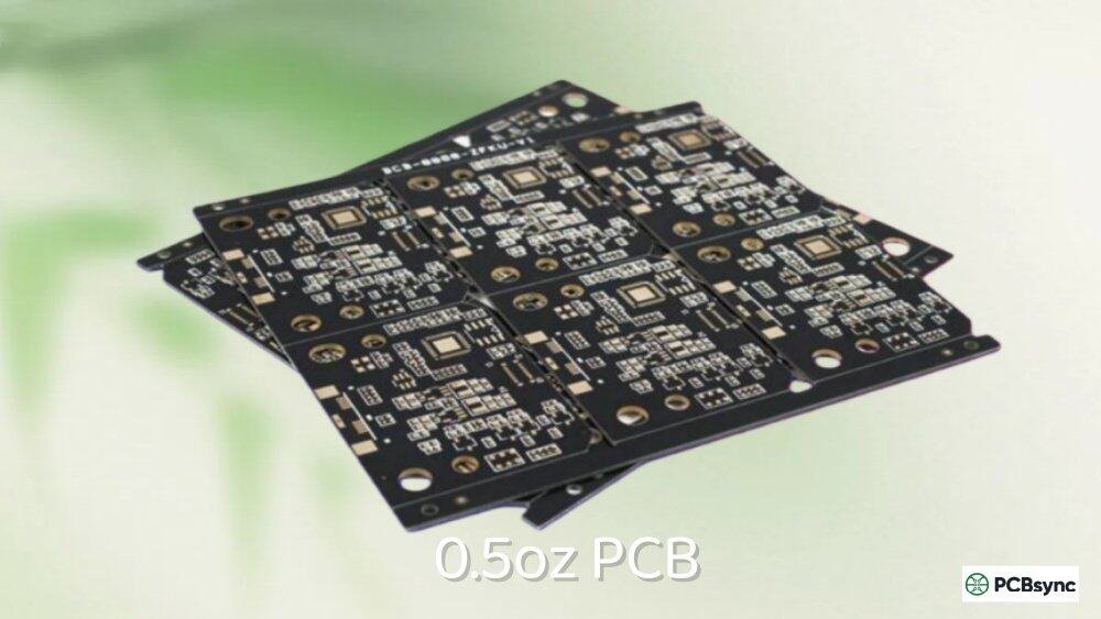
If you’ve ever wondered exactly how thick 0.5 oz copper thickness actually is, you’re not alone. This specification appears constantly in PCB stack-ups, fabricator quotes, and design guidelines—yet the conversion from ounces to actual dimensions trips up even experienced engineers.
Here’s the quick answer: 0.5 oz copper equals approximately 17-18 micrometers (0.7 mils). But there’s much more to understand about when and why to use half-ounce copper in your designs.
This guide covers everything from precise conversions to practical applications, helping you make informed decisions about copper weight selection for your next PCB project.
0.5 oz copper thickness refers to copper foil weighing half an ounce per square foot of area. When this copper is spread uniformly across that square foot, it produces a layer approximately 17-18 micrometers thick.
The ounce-based measurement system originated decades ago when copper foil suppliers found that weighing copper sheets was more practical than measuring their thickness directly. Since copper density is constant, weight directly correlates to thickness—and the convention stuck.
Why Ounces Instead of Microns?
It seems counterintuitive to specify thickness using a weight measurement. If someone asked your height and you answered “180 pounds,” they’d think you were confused. Yet in the PCB industry, copper thickness has been specified by weight for generations.
The practical reason: copper foil surfaces have microscopic texture and treatment variations that make direct thickness measurement inconsistent. Weighing a standardized area provides a reliable, repeatable specification that material suppliers, fabricators, and designers all understand.
Engineers need to work in various unit systems depending on their tools and region. Here’s a comprehensive conversion table for 0.5 oz copper:
Unit
0.5 oz Copper Value
Notes
Micrometers (μm)
17-18 μm
Nominal specification
Mils
0.7 mils
Common in US specifications
Millimeters (mm)
0.018 mm
Metric equivalent
Inches
0.0007 inches
Rarely used directly
Microns (actual)
~15 μm
After processing per IPC
The IPC Reality Check
Here’s something many engineers don’t realize: the nominal 0.5 oz copper thickness (17-18 μm) isn’t what you actually get on a finished board.
According to IPC-4562A (Metal Foil for Printed Board Applications), PCB manufacturing tolerances and processing steps reduce the actual copper thickness. For inner layers, 0.5 oz copper typically measures around 15 μm (0.6 mils) after fabrication. The Z-zero stackup analysis team reports seeing this value on approximately 95% of fabricator stackups.
This matters for impedance calculations. If your EDA tool assumes 18 μm but the fabricator delivers 15 μm, your controlled impedance traces will be slightly off-target.
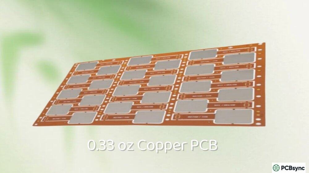
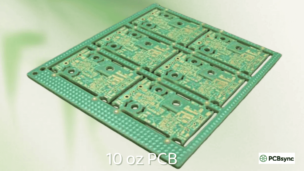
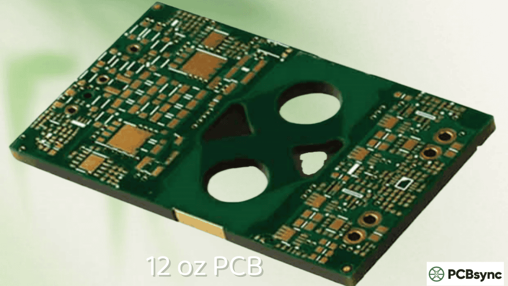
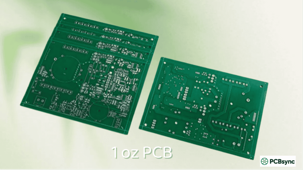
0.5 oz vs 1 oz Copper Thickness Comparison
The choice between 0.5 oz and 1 oz copper is one of the most common decisions PCB designers face. Here’s how they compare:
Parameter
0.5 oz Copper
1 oz Copper
Nominal Thickness
17-18 μm
34-35 μm
Actual Thickness (IPC)
~15 μm
~30 μm
Thickness in Mils
0.7 mils
1.4 mils
Sheet Resistance
~1.1 mΩ/sq
~0.55 mΩ/sq
Minimum Trace Width
3 mil (75 μm)
4 mil (100 μm)
Minimum Spacing
3 mil (75 μm)
4 mil (100 μm)
Relative Cost
Lower
Standard
Flexibility
Better
Good
Electrical Differences
The DC resistance of 0.5 oz copper is exactly double that of 1 oz copper for identical trace geometries. For signal traces carrying milliamps, this difference is negligible. For power distribution carrying amps, it matters significantly.
Consider a 10-mil wide trace carrying 500mA:
With 1 oz copper: approximately 13 mΩ per inch of trace length
With 0.5 oz copper: approximately 26 mΩ per inch of trace length
Over a 6-inch power trace, that’s the difference between 78 mΩ and 156 mΩ total resistance—and corresponding voltage drops of 39 mV versus 78 mV at 500mA.
When the Difference Doesn’t Matter
For most signal routing applications, the electrical distinction between 0.5 oz and 1 oz copper is negligible. Digital signals, low-frequency analog, and communication interfaces all work fine with either thickness.
The choice becomes significant when:
Distributing power across long traces
Operating at elevated temperatures
Designing for high-current applications
Optimizing for fine-pitch routing
Applications for 0.5 oz Copper Thickness
Half-ounce copper serves specific purposes in PCB design. Understanding these applications helps you select the right copper weight for your project.
Inner Layers of Multilayer PCBs
The most common application for 0.5 oz copper is on inner signal layers of multilayer boards. Many standard 4-layer and 6-layer stack-ups specify:
Outer layers: 1 oz copper (for component pads and power)
Inner layers: 0.5 oz copper (for signal routing)
This combination balances manufacturability, cost, and performance. The thinner inner layer copper enables finer traces for dense signal routing, while the thicker outer layers provide robust pads for assembly.
Layer 1 (Top): 1 oz copper – Components and signals
Layer 2 (Inner): 0.5 oz copper – Ground plane
Layer 3 (Inner): 0.5 oz copper – Power plane or signals
Layer 4 (Bottom): 1 oz copper – Components and signals
Flexible Circuit Boards
Flex PCBs commonly use 0.5 oz copper because thinner copper bends more easily without cracking. The relationship between copper thickness and flex life is significant—doubling copper thickness can reduce bend cycles to failure by more than half.
For dynamic flex applications (circuits that bend repeatedly during operation), 0.5 oz or even thinner copper is often mandatory. Static flex applications (bent once during assembly) can sometimes use 1 oz copper, but 0.5 oz remains popular for its superior flexibility.
Fine-Line and HDI Designs
When your design requires traces below 4 mils (100 μm), thinner copper becomes necessary for reliable etching. The etching process removes copper not just vertically but also laterally (undercut), and this lateral etching increases with copper thickness.
With 0.5 oz copper, fabricators can reliably produce:
3 mil traces and spaces (standard capability)
2.5 mil traces and spaces (advanced capability)
Achieving these dimensions with 1 oz copper is significantly more challenging and may require specialized processing.
Consumer Electronics
Cost-sensitive consumer products often specify 0.5 oz copper on inner layers to reduce material costs. The copper foil itself is less expensive, and the thinner copper can reduce overall board thickness—important for slim devices like smartphones and tablets.
Signal Integrity Applications
For controlled impedance designs, 0.5 oz copper can actually improve consistency. Thinner copper has less variation in thickness across the panel, leading to more predictable impedance values. This is particularly valuable for high-speed digital and RF designs where impedance tolerance is tight.
Current Carrying Capacity at 0.5 oz Copper Thickness
Understanding how much current your traces can safely carry is critical for reliable designs. The IPC-2221 standard provides guidelines, but the values for 0.5 oz copper are often harder to find than for 1 oz.
Current Capacity Guidelines
Current capacity depends on trace width, copper thickness, allowable temperature rise, and whether the trace is on an outer layer (better cooling) or inner layer (worse cooling).
Trace Width
0.5 oz External (10°C rise)
0.5 oz Internal (10°C rise)
5 mil
0.35 A
0.18 A
10 mil
0.55 A
0.28 A
20 mil
0.90 A
0.45 A
50 mil
1.60 A
0.80 A
100 mil
2.50 A
1.25 A
Note: Internal traces have approximately half the current capacity of external traces due to reduced heat dissipation.
Temperature Rise Considerations
The values above assume a 10°C temperature rise above ambient. If your application can tolerate higher temperature rise, current capacity increases:
20°C rise: approximately 1.5x the 10°C values
30°C rise: approximately 1.8x the 10°C values
However, higher operating temperatures accelerate board aging and may affect nearby components. Most designs target 10-20°C rise as a reasonable compromise.
IPC-2152 vs IPC-2221
The older IPC-2221 standard tends to be conservative compared to the newer IPC-2152. For critical applications, IPC-2152 provides more detailed analysis methods that account for factors like nearby copper (heat spreading), board thickness, and thermal vias.
Successfully designing with half-ounce copper requires understanding its capabilities and limitations.
Trace Width and Spacing Rules
Thinner copper enables finer features, but you still need to respect manufacturing limits:
Feature
0.5 oz Copper Capability
1 oz Copper Capability
Minimum Trace Width
3 mil (75 μm)
4 mil (100 μm)
Minimum Spacing
3 mil (75 μm)
4 mil (100 μm)
Typical Trace/Space
4/4 mil
5/5 mil
Fine-Line Trace/Space
3/3 mil
4/4 mil
These are general guidelines—verify with your specific fabricator, as capabilities vary.
Impedance Calculation Adjustments
When calculating controlled impedance for 0.5 oz copper:
Use actual thickness (15 μm) rather than nominal (18 μm)
Account for trapezoidal trace cross-section from etching
Verify assumptions with your fabricator’s impedance calculator
A microstrip trace designed for 50Ω with 1 oz copper assumptions may measure 52-53Ω when fabricated with 0.5 oz copper if thickness isn’t correctly specified.
Power Distribution Strategies
If your design includes both signal routing (suitable for 0.5 oz) and power distribution (better with heavier copper), consider these strategies:
Mixed copper weights: Specify different copper weights on different layers. Inner signal layers can be 0.5 oz while outer layers or dedicated power layers use 1 oz or heavier.
Wider power traces: Compensate for thinner copper by increasing trace width. Doubling trace width provides the same cross-sectional area (and current capacity) as doubling copper thickness.
Parallel traces: Route power on multiple layers in parallel, connected by vias, to increase effective copper cross-section.
Stack-up Symmetry
For multilayer boards, maintain symmetric copper weights above and below the board’s center line. This prevents warping during thermal cycling:
Good (symmetric):
L1: 1 oz
L2: 0.5 oz
L3: 0.5 oz
L4: 1 oz
Poor (asymmetric):
L1: 1 oz
L2: 1 oz
L3: 0.5 oz
L4: 0.5 oz
Manufacturing Considerations
Understanding how fabricators handle 0.5 oz copper helps you design boards that manufacture reliably.
Material Availability
Most PCB fabricators stock 0.5 oz copper foil or can readily obtain it. It’s a standard option, not a specialty material. However, lead times may be slightly longer than for 1 oz copper if the fabricator doesn’t keep 0.5 oz in their standard inventory.
Etching Process
Thinner copper etches faster and with less undercut, enabling finer features. The etching time for 0.5 oz copper is roughly half that of 1 oz copper, which can actually improve yield on fine-pitch designs by reducing over-etching.
Plating Considerations
Outer layer copper thickness increases during the plating process. Starting with 0.5 oz base copper, the finished outer layer thickness after plating typically reaches 1.0-1.2 oz equivalent (35-42 μm).
This plating addition affects:
Final trace dimensions (traces become slightly wider)
Using 0.5 oz copper on inner layers instead of 1 oz typically reduces board cost by 5-15%, depending on the fabricator and layer count. The savings come from:
Lower material cost for thinner copper foil
Faster etching (improved throughput)
Better yield on fine-pitch designs
Useful Resources for 0.5 oz Copper PCB Design
IPC Standards
IPC-2221: Generic Standard on Printed Board Design (current capacity charts)
IPC-2152: Standard for Determining Current-Carrying Capacity in Printed Board Design
IPC-4562A: Metal Foil for Printed Board Applications (copper specifications)
IPC-6012: Qualification and Performance Specification for Rigid Printed Boards
Online Calculators
Saturn PCB Toolkit: Free comprehensive calculator including trace width, impedance, and current capacity
Sierra Circuits Trace Width Calculator: Web-based tool for current capacity analysis
Altium Designer Built-in Calculator: Integrated into the design environment
Most PCB fabricators publish their standard stack-ups online, showing typical copper weight configurations:
Check your fabricator’s design guidelines
Request impedance modeling for your specific stack-up
Verify actual copper thickness values used in their calculations
Frequently Asked Questions About 0.5 oz Copper Thickness
How thick is 0.5 oz copper in mm and mils?
0.5 oz copper thickness equals approximately 0.018 mm or 0.7 mils nominally. However, per IPC standards, the actual thickness after processing is closer to 0.015 mm (15 μm) or 0.6 mils. When performing impedance calculations or stack-up analysis, use the actual processed thickness rather than the nominal value for accurate results. Most fabricator stack-up documents will specify which value they use.
What is the current carrying capacity of 0.5 oz copper traces?
Current capacity depends on trace width, location (inner vs outer layer), and acceptable temperature rise. As a general guideline, a 10-mil wide trace on 0.5 oz copper can carry approximately 0.55A on an external layer or 0.28A on an internal layer with a 10°C temperature rise. For higher currents, increase trace width or use heavier copper. Always verify designs using IPC-2152 guidelines or online calculators for your specific configuration.
Should I use 0.5 oz or 1 oz copper for my PCB design?
Choose 0.5 oz copper when you need fine-pitch routing (traces below 4 mils), are designing flex circuits requiring good bend performance, want to reduce costs on inner signal layers, or are working on HDI designs. Choose 1 oz copper when carrying significant current (over 0.5A per trace), designing power distribution layers, or when your fabricator’s standard stack-up uses 1 oz. Many designs use both: 0.5 oz on inner signal layers and 1 oz on outer layers.
Does 0.5 oz copper affect controlled impedance?
Yes, copper thickness directly affects impedance calculations. Thinner copper (0.5 oz) generally requires slightly narrower traces to achieve the same impedance as thicker copper (1 oz) in microstrip configurations. More importantly, ensure your impedance calculations use the correct actual thickness value (~15 μm for 0.5 oz) rather than nominal values. Work with your fabricator to verify their impedance modeling assumptions match your design intent.
Is 0.5 oz copper suitable for flex PCBs?
0.5 oz copper is excellent for flex PCBs and is often the preferred choice. Thinner copper provides better flexibility and longer flex life compared to 1 oz copper. For dynamic flex applications where the circuit bends repeatedly, 0.5 oz or thinner copper is typically required to prevent copper cracking. For static flex applications (bent only during installation), either 0.5 oz or 1 oz can work, but 0.5 oz provides additional margin for reliability.
Summary: When to Specify 0.5 oz Copper Thickness
0.5 oz copper thickness occupies an important middle ground in PCB design—thinner than the ubiquitous 1 oz standard but thicker than ultra-thin foils used in advanced HDI. At 17-18 μm nominal (15 μm actual), it enables finer traces than 1 oz copper while maintaining good manufacturability and reasonable current capacity.
Power distribution layers carrying significant current
The right copper weight depends on your specific application requirements. Understanding the capabilities and limitations of 0.5 oz copper thickness helps you make informed decisions that balance performance, manufacturability, and cost for your PCB designs.
Inquire: Call 0086-755-23203480, or reach out via the form below/your sales contact to discuss our design, manufacturing, and assembly capabilities.
Quote: Email your PCB files to Sales@pcbsync.com (Preferred for large files) or submit online. We will contact you promptly. Please ensure your email is correct.
Notes: For PCB fabrication, we require PCB design file in Gerber RS-274X format (most preferred), *.PCB/DDB (Protel, inform your program version) format or *.BRD (Eagle) format. For PCB assembly, we require PCB design file in above mentioned format, drilling file and BOM. Click to download BOM template To avoid file missing, please include all files into one folder and compress it into .zip or .rar format.


