Inquire: Call 0086-755-23203480, or reach out via the form below/your sales contact to discuss our design, manufacturing, and assembly capabilities.
Quote: Email your PCB files to Sales@pcbsync.com (Preferred for large files) or submit online. We will contact you promptly. Please ensure your email is correct.
Notes: For PCB fabrication, we require PCB design file in Gerber RS-274X format (most preferred), *.PCB/DDB (Protel, inform your program version) format or *.BRD (Eagle) format. For PCB assembly, we require PCB design file in above mentioned format, drilling file and BOM. Click to download BOM template To avoid file missing, please include all files into one folder and compress it into .zip or .rar format.
Understanding what goes into a printed circuit board (PCB) is essential for engineers, designers, and anyone working in electronics manufacturing. From the copper-clad core to the protective solder mask, each layer serves a critical purpose. This comprehensive guide breaks down every PCB material and component you need to know.
What Is a PCB Made Of? The Basic Structure
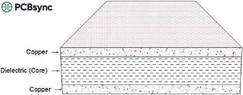
At its foundation, a PCB consists of copper-clad fiberglass material—thin copper sheets bonded to either side of a rigid board. For multilayer PCBs (boards with more than two copper layers), manufacturers use Pre-Preg material between core layers to create a single, unified board with multiple conductive layers.
Core Materials: The Foundation of Every PCB
Core material is a rigid sheet of fiberglass resin with copper sheets adhered to one or both sides. The copper thickness is measured in ounces (oz), which translates to specific thicknesses used during board lay-up.
Standard Copper Thickness by Weight
½ oz copper: 0.0007″ (0.0178mm) — ideal for fine-pitch designs
1 oz copper: 0.0014″ (0.0356mm) — standard for most applications
2 oz copper: 0.0028″ (0.0711mm) — for high-current applications
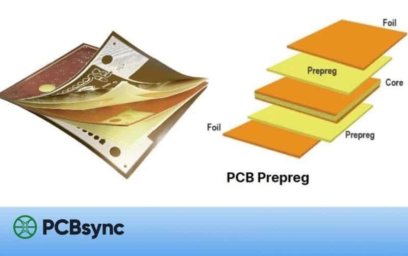
Pre-Preg: The Bonding Agent for Multilayer PCBs
Pre-Preg (pre-impregnated) material shares similar composition with core material but comes in a soft, pliable form with built-in adhesive properties. These thin sheets are stacked to achieve custom thicknesses during the lamination process.
Common Pre-Preg Thicknesses
0.002″ (0.0508mm)
0.003″ (0.0762mm)
0.004″ (0.1016mm)
Pro Tip: When calculating stack-up thickness, use multiples of 0.002″ or standard combinations for best results.
Copper Foil and Copper Plating: Building Conductivity
Copper Foil
Copper foil is a thin copper sheet placed on or between Pre-Preg materials. The adhesive properties of Pre-Preg bond the foil during lamination. Standard copper foil thicknesses match those used in core materials: ½ oz, 1 oz, and 2 oz.
Copper Plating
Applied primarily to external layers, copper plating serves two critical functions: adding thickness to external traces and plating the walls of drilled holes. The average plating thickness ranges from 0.0012″ to 0.0014″ (0.0304–0.0356mm). This hole wall plating creates electrical connections between layers.
Surface Finishes: Solder Flow and SMOBC
Solder flow applies molten solder to exposed copper areas on the board’s external surfaces. This process prepares the board for component assembly and protects copper from oxidation. Two approaches exist: full-board solder flow or SMOBC (Solder Mask Over Bare Copper), where only designated pads and soldering areas receive the solder coating.
Solder Mask: The Protective Layer
Solder mask is the colored coating (typically green) applied to PCB surfaces. It provides multiple protective functions:
Environmental protection against moisture and contaminants
Electrical insulation between traces
Prevention of solder bridges during assembly
Physical protection for mounted components
Heat dissipation from active components
Note: Some industry standards do not consider solder mask an adequate insulator due to inconsistent thickness and material variations between manufacturers.
PCB Traces: The Copper Highways
A trace functions as a wire embedded in the PCB, conducting electricity between connection points. During manufacturing, an etching process removes unwanted copper, leaving only the required traces and pads.
Trace Width Guidelines
The current-carrying capacity of a trace depends on its width, thickness, and location (internal vs. external). General guidelines include:
External traces: 0.010″ per 1 Amp (typically 1.5 oz copper)
Internal traces: 0.040″ per 1 Amp (typically ½ oz copper)
Accurate trace sizing requires calculations that account for temperature rise, current load, trace width, copper thickness, and layer location. Design software with built-in calculators provides the most reliable results.
PCB Pads: Connection Points for Components
Pads provide the mounting and electrical connection points for components. Two primary types exist: surface-mount pads (flat copper areas for SMD components) and through-hole pads (pads with holes for leaded components). Component manufacturers typically specify recommended pad dimensions for their parts.
Plated through-holes feature copper-plated walls that extend from surface pads into the hole, creating reliable electrical connections. PTH technology offers several advantages:
Enables smaller pad sizes due to structural support
Improves heat dissipation during soldering
Provides top-to-bottom layer connectivity regardless of component insertion
Enables solder flow through the hole, eliminating double-sided soldering
Essential for internal layer connections in multilayer boards
Non-Plated Through-Holes (NPTH): Mechanical Features
Non-plated holes lack copper plating on their walls and typically serve mechanical purposes—mounting hardware, alignment pins, or ventilation. A clearance area around NPTH prevents shorting between inserted objects and copper layers. Boards without plated holes skip the plating process, reducing cost but requiring larger pads and limiting design options.
Slots and Cutouts: Custom Board Shapes
Unlike drilled circular holes, slots and cutouts are created using router bits, producing oval, oblong, or rounded rectangular shapes. Since router bits are round, internal corners have a minimum radius equal to the bit radius. Smaller bits on thicker boards require slower cutting speeds, increasing manufacturing time and cost.
Board Edge Considerations
The board edge encompasses any area exposing the PCB’s cross-section—including the outer perimeter, slots, and cutouts. Edge specifications affect manufacturability, clearance requirements, and assembly compatibility. Proper edge clearance prevents damage during handling and ensures reliable operation.
Key Takeaways
Understanding PCB materials enables better design decisions and clearer communication with manufacturers. Whether you’re specifying copper weights, calculating trace widths, or selecting surface finishes, this knowledge forms the foundation for successful PCB projects. For complex designs, always consult with your fabrication partner early in the process to optimize material selection and ensure manufacturability.
Inquire: Call 0086-755-23203480, or reach out via the form below/your sales contact to discuss our design, manufacturing, and assembly capabilities.
Quote: Email your PCB files to Sales@pcbsync.com (Preferred for large files) or submit online. We will contact you promptly. Please ensure your email is correct.
Notes: For PCB fabrication, we require PCB design file in Gerber RS-274X format (most preferred), *.PCB/DDB (Protel, inform your program version) format or *.BRD (Eagle) format. For PCB assembly, we require PCB design file in above mentioned format, drilling file and BOM. Click to download BOM template To avoid file missing, please include all files into one folder and compress it into .zip or .rar format.


