Inquire: Call 0086-755-23203480, or reach out via the form below/your sales contact to discuss our design, manufacturing, and assembly capabilities.
Quote: Email your PCB files to Sales@pcbsync.com (Preferred for large files) or submit online. We will contact you promptly. Please ensure your email is correct.
Notes: For PCB fabrication, we require PCB design file in Gerber RS-274X format (most preferred), *.PCB/DDB (Protel, inform your program version) format or *.BRD (Eagle) format. For PCB assembly, we require PCB design file in above mentioned format, drilling file and BOM. Click to download BOM template To avoid file missing, please include all files into one folder and compress it into .zip or .rar format.
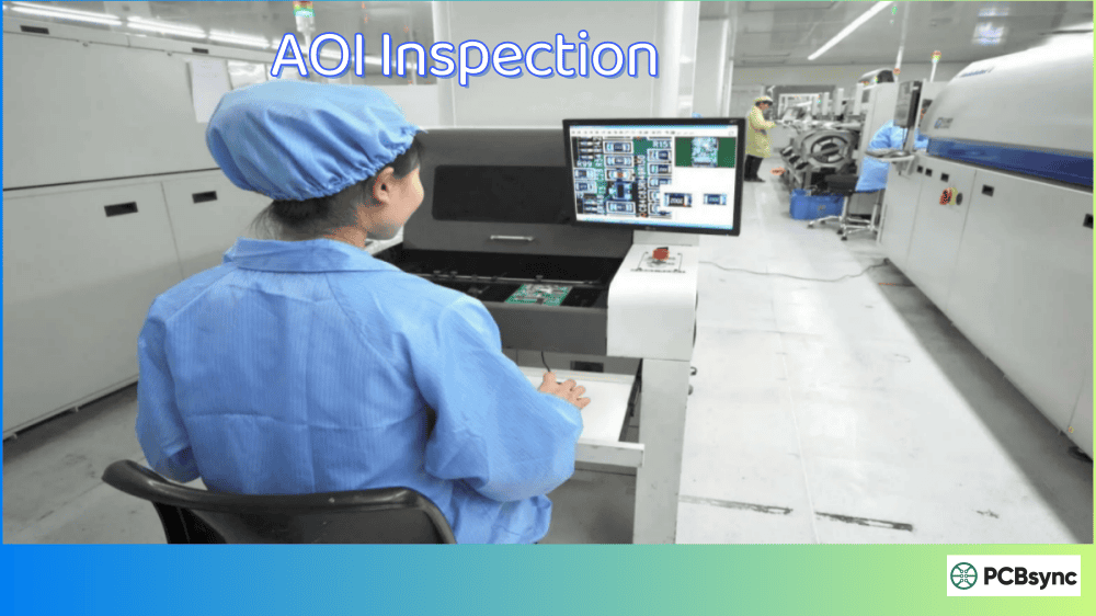
If you’ve spent any time on a modern SMT line, you know that manual inspection simply doesn’t cut it anymore. With component sizes shrinking to 01005 packages and board densities hitting record highs, the human eye can’t keep up. That’s where automated optical inspection comes into play—and honestly, it’s become the backbone of quality control in every serious PCB manufacturing operation I’ve worked with.
In this guide, I’ll walk you through everything you need to know about AOI systems, from basic principles to advanced implementation strategies. Whether you’re evaluating your first AOI machine or optimizing an existing setup, this information comes from real-world experience on production floors.
Automated optical inspection (AOI) is a machine vision-based technology that uses high-resolution cameras and sophisticated image processing algorithms to inspect printed circuit boards for manufacturing defects. The system captures images of the PCB and compares them against a reference standard—either a “golden board” or CAD data—to identify anomalies.
Think of AOI as having hundreds of trained inspectors working simultaneously, except they never get tired, never miss a shift, and can examine thousands of solder joints per second with sub-pixel accuracy. In my experience, a good AOI system catches defects that even experienced technicians would miss, especially on densely populated boards.
The Core Technology Behind AOI Systems
Every automated optical inspection system consists of four fundamental components working together:
Imaging System: High-resolution cameras (typically ranging from 5 to 25 megapixels) capture detailed images of the PCB surface. Modern systems often use multiple cameras positioned at different angles to eliminate blind spots caused by component shadows.
Lighting Architecture: This is more critical than most people realize. AOI machines use configurable LED arrays in red, green, blue, and white colors, positioned at various angles (top-down, low-angle, side-angle) to highlight different defect types. The lighting setup can make or break your detection rates.
Image Processing Engine: Advanced algorithms analyze captured images, performing pattern matching, edge detection, and dimensional measurements. Many newer systems incorporate AI and machine learning to improve accuracy over time.
Conveyor and Positioning System: Precision mechanics move the board through the inspection zone with positional accuracy better than ±0.02mm—essential when you’re looking at component placements measured in micrometers.
How Automated Optical Inspection Works
The inspection process follows a logical sequence that any process engineer should understand:
Step 1: Image Acquisition
When a PCB enters the AOI machine, the system activates its lighting modules in a programmed sequence. Different lighting angles reveal different features—low-angle lighting highlights solder fillet profiles, while top-down illumination works better for component markings and polarity indicators.
The cameras capture multiple images of each inspection area, often using various lighting conditions in rapid succession. A typical AOI system might take 20-30 images per field of view, each optimized for detecting specific defect types.
Step 2: Image Processing and Analysis
Here’s where the real magic happens. The software compares each captured image against reference data using several techniques:
Pattern Matching: The system looks for expected shapes, sizes, and positions of components. Any deviation beyond programmed tolerances gets flagged.
Color Analysis: Solder joints have characteristic color signatures based on their quality. Good joints reflect light differently than cold joints or those with insufficient solder.
Dimensional Measurement: The software calculates actual measurements—fillet height, component offset, rotation angle—and compares them against specifications.
Presence Verification: Simple but critical—confirming that every component is actually there.
Step 3: Defect Classification and Reporting
Detected anomalies get classified by type and severity. Modern systems provide real-time statistical process control (SPC) data, showing defect trends that help identify upstream issues before they cause major problems.
2D AOI vs 3D AOI: Understanding the Differences
One of the most common questions I get is whether to invest in 2D or 3D automated optical inspection. The answer depends on your specific production requirements.
2D AOI Technology
Traditional 2D AOI systems capture flat, top-down images of the PCB. They’re excellent for detecting:
Missing or wrong components
Polarity errors
Solder bridges visible from above
Component offset and rotation
Text and marking verification
2D systems cost less and run faster, making them ideal for high-volume production of relatively simple boards. However, they struggle with height-related defects and anything hidden by component shadows.
3D AOI Technology
3D AOI uses structured light projection, laser scanning, or phase-shift Moiré technology to capture actual height information. This enables detection of:
Lifted leads and tombstoning
Coplanarity issues
Solder volume measurement
Head-in-pillow defects
Accurate fillet analysis
The following table summarizes the key differences:
Feature
2D AOI
3D AOI
Height Measurement
No
Yes
Solder Volume Analysis
Limited
Accurate
Inspection Speed
Faster
Slightly Slower
Equipment Cost
$30,000 – $80,000
$80,000 – $250,000+
Best Application
Standard SMT boards
Complex assemblies, BGA-heavy designs
False Call Rate
Higher
Lower
Lifted Lead Detection
Poor
Excellent
For most operations running boards with BGAs, QFNs, or fine-pitch components, 3D AOI provides significantly better value despite the higher upfront cost. The reduction in false calls alone often justifies the investment.
Where to Position AOI in Your SMT Line
Strategic placement of automated optical inspection equipment dramatically impacts its effectiveness. There are four common positions, each serving different purposes.
Post-Paste (SPI Integration)
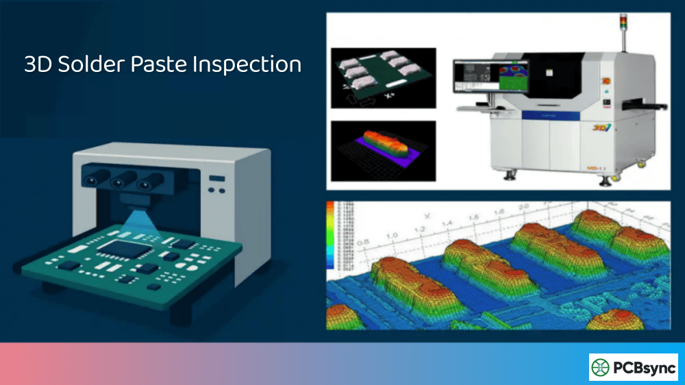
While technically not AOI but rather Solder Paste Inspection (SPI), this position catches stencil printing defects before any components are placed. Issues like insufficient paste, bridging, or offset deposits get caught immediately.
Pre-Reflow Inspection
Placing AOI after pick-and-place but before reflow soldering catches component placement errors when rework is easiest—components can simply be repositioned or replaced without desoldering. Defects detected here include:
Missing components
Wrong parts
Polarity errors
Placement offset
Tombstoning risk (lifted components)
Post-Reflow Inspection
This is the most common AOI position because it provides comprehensive inspection of the finished assembly. Post-reflow AOI can detect virtually all visible defects in a single pass:
For through-hole components processed through wave or selective soldering, additional AOI inspection catches solder joint defects specific to these processes.
Hidden solder joints: Connections under BGAs, QFNs, and other bottom-terminated components require X-ray inspection
Internal PCB defects: Delamination, internal shorts, and via issues aren’t visible optically
Certain solder voids: Surface voids might be visible, but internal voids require AXI
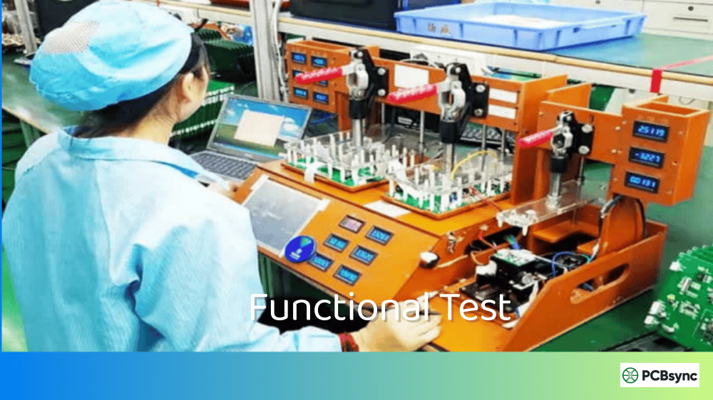
Functional defects: AOI doesn’t test electrical function—that requires ICT or functional testing
AOI vs X-Ray Inspection (AXI): Which Do You Need?
This comparison comes up constantly, so let me be clear: AOI and AXI aren’t competitors—they’re complementary technologies.
Aspect
Automated Optical Inspection (AOI)
Automated X-Ray Inspection (AXI)
Inspection Method
Visible light imaging
X-ray penetration imaging
What It Sees
Surface features only
Internal and hidden structures
Best For
Surface-mount components, visible solder joints
BGAs, QFNs, hidden solder joints, voids
Speed
10-30 seconds per board typical
1-5 minutes per board typical
Cost
Lower ($30K-$250K)
Higher ($150K-$500K+)
Throughput
High-volume compatible
Better for sampling or critical boards
Operator Skill
Moderate
Higher (X-ray image interpretation)
When to use AOI: Every board should pass through AOI. It’s your first line of defense and catches 70-80% of assembly defects.
When to add AXI: If your design includes BGAs, QFNs, chip-scale packages, or other components with hidden solder connections, AXI becomes essential—at least for sampling inspection.
Many facilities use both: 100% AOI inspection with statistical AXI sampling on boards containing hidden-joint components.
Programming Your AOI System
Getting reliable results from automated optical inspection requires proper programming. There are two main approaches:
Golden Board Method
The traditional approach uses a known-good PCB assembly as the reference:
Run a verified board through the AOI
Let the system learn component appearances and positions
Teach acceptable variation ranges through multiple sample boards
Fine-tune thresholds based on initial production runs
Pros: Fast setup, intuitive process Cons: Requires good samples, may miss systematic defects present on “golden” board
IPC-A-610 defines three product classes that determine inspection stringency:
Class 1: General Electronic Products
Consumer electronics, non-critical applications
Most relaxed acceptance criteria
Class 2: Dedicated Service Electronic Products
Industrial equipment, telecom, computers
Moderate reliability requirements
Class 3: High-Performance Electronic Products
Medical devices, aerospace, military
Highest reliability, strictest inspection
Your AOI programming should align with the appropriate IPC class for your products. Class 3 assemblies require tighter tolerances and more comprehensive inspection coverage.
Best Practices for AOI Implementation
After implementing AOI systems across multiple facilities, here’s what consistently works:
Start With Realistic Expectations
AOI isn’t magic—it catches what it’s programmed to catch. Invest time in proper setup and don’t expect perfection on day one.
Train Your Operators
The best AOI system fails with poorly trained operators. Ensure your team understands:
How to verify and classify flagged defects
When to adjust thresholds vs. when to escalate
Basic troubleshooting for common issues
Integrate With Your Process
AOI data is incredibly valuable for process improvement. Use it to:
Track defect trends over time
Identify problematic components or placements
Verify process changes
Support root cause analysis
Maintain Your Equipment
Regular maintenance prevents drift and downtime:
Clean cameras and lighting daily
Verify calibration weekly
Service conveyor systems per manufacturer schedule
Update software when stable releases are available
Balance Speed and Coverage
There’s always tension between throughput and inspection completeness. Work with your quality team to determine:
Which defects are critical vs. minor
Where 100% inspection is required vs. sampling acceptable
Optimal cycle time targets
Useful Resources for AOI Implementation
Industry Standards and Documentation
IPC-A-610 (Current revision): Essential reference for acceptance criteria – Available at IPC.org
AOI Equipment Manufacturers: Koh Young, Mirtec, Omron, Viscom, and others publish application notes and technical guides
IPC EDGE Online Training: Self-paced courses on inspection standards
ResearchGate: Academic papers on AOI algorithms and machine learning applications
Component Databases
SiliconExpert: Component specifications and lifecycle data
Octopart: Component search and datasheet access
IPC-7351: Land pattern standards for component libraries
Frequently Asked Questions
What is the typical accuracy of modern AOI systems?
Modern 3D AOI systems achieve detection rates of 98-99% for surface-visible defects, with false call rates below 100 ppm when properly programmed. 2D systems typically show slightly higher false call rates due to limitations in height measurement. The key factor isn’t the machine specification—it’s the quality of your programming and maintenance.
How does AOI differ from manual visual inspection?
Manual inspection using magnification can examine 500-800 components per hour with accuracy around 85-90%, heavily dependent on inspector fatigue and skill level. Automated optical inspection examines 5,000+ components per hour with consistent 98%+ accuracy. More importantly, AOI provides objective, repeatable measurements and generates data for process improvement—something manual inspection cannot match.
Can AOI detect defects under BGA components?
No. Standard AOI systems only see surface features visible to cameras. Ball Grid Array solder joints are completely hidden under the package body. For BGA inspection, you need either X-ray inspection (AXI) or specialized techniques like boundary scan testing. This is why many facilities use AOI and AXI together—AOI for visible defects, AXI for hidden connections.
What factors affect AOI inspection time per board?
Several factors influence cycle time: board size (larger boards take longer), component density (more inspection points), inspection coverage level (100% vs. sampling), image resolution settings, number of lighting conditions used per location, and defect verification requirements. A typical mid-complexity board runs 15-30 seconds through modern AOI systems.
How often should AOI systems be calibrated?
Most manufacturers recommend formal calibration verification weekly, with full calibration monthly or quarterly depending on production volume. However, you should verify calibration immediately after any maintenance, software updates, or if you notice unusual false call patterns. Daily cleaning of cameras and lighting is essential for consistent performance between calibrations.
Advanced AOI Features and Emerging Technologies
The automated optical inspection landscape continues evolving rapidly. Understanding these advances helps you make informed investment decisions.
AI and Machine Learning Integration
Traditional AOI relies on rule-based algorithms—if a measurement exceeds threshold X, flag it as a defect. This approach works but generates false calls when encountering acceptable variations the programmer didn’t anticipate.
Machine learning changes this equation fundamentally. Modern AOI systems learn from operator verification decisions, automatically adjusting their internal models to distinguish real defects from acceptable variations. After processing thousands of boards, these systems achieve false call rates that rule-based systems simply cannot match.
Some specific applications of AI in automated optical inspection include:
Adaptive Threshold Learning: The system observes which flagged items operators verify as real defects versus false calls, then adjusts thresholds automatically.
Defect Classification: Rather than just detecting anomalies, AI systems categorize defects by type, severity, and probable cause—invaluable for root cause analysis.
Process Drift Detection: Machine learning algorithms identify subtle trends that indicate process drift before it causes defect escapes.
Smart Factory Integration
Industry 4.0 connectivity transforms AOI from standalone inspection to integrated process control. Modern systems communicate directly with:
Solder paste printers (adjusting stencil alignment based on SPI data)
Symptoms: Defects found at downstream inspection or customer returns
Investigation Steps:
Verify the defect type should be detectable by AOI (not hidden joints)
Check if the defect location was included in inspection coverage
Review lighting conditions for that component area
Examine threshold settings—may be too loose
Verify camera resolution is adequate for the defect size
Inconsistent Results
Symptoms: Same defect flagged sometimes but not others
Common Causes:
Board positioning variation—check conveyor guides and stops
Lighting intensity fluctuation—LEDs degrade over time
Temperature affecting camera performance—verify environmental controls
Software version inconsistency across shifts—standardize updates
Calculating AOI Return on Investment
Justifying AOI investment requires understanding both costs and benefits.
Cost Factors
Initial Investment: Equipment purchase ($30K-$250K+ depending on capability), installation, programming, and training.
Ongoing Costs: Maintenance contracts (typically 5-10% of purchase price annually), consumables, calibration, software updates, and floor space.
Benefit Calculation
Direct Savings:
Reduced manual inspection labor
Lower rework costs through earlier defect detection
Decreased scrap from catching defects before additional processing
Indirect Benefits:
Customer satisfaction improvement
Warranty claim reduction
Process improvement from data analysis
Reduced inspection variation
Sample ROI Calculation
For a facility producing 500 boards per day with manual inspection costing $25/hour:
Factor
Before AOI
After AOI
Inspection labor (hrs/day)
16
2
Daily labor cost
$400
$50
Defect escape rate
2%
0.3%
Rework cost per escape
$50
$50
Daily escape cost
$500
$75
Total daily cost
$900
$125
Annual savings: ($900 – $125) × 250 working days = $193,750
With an AOI investment of $100,000, payback occurs in approximately 6 months—and that doesn’t include the harder-to-quantify benefits of improved customer satisfaction and process data.
Taking Your AOI Program to the Next Level
Automated optical inspection has evolved from a nice-to-have into an absolute necessity for competitive PCB manufacturing. With component sizes continuing to shrink and board complexity increasing, the technology will only become more critical.
The manufacturers getting the best results treat AOI not just as a gate to catch defects, but as a process monitoring tool that drives continuous improvement. When you analyze your AOI data properly, it tells you exactly where your process needs attention—before defects become customer complaints.
If you’re just starting with AOI, invest in proper training and don’t rush the programming phase. If you’ve had AOI for years, challenge whether you’re actually using all the data it generates. The boards going through your line every day are telling you exactly how to improve—you just need to listen.
The future of automated optical inspection points toward greater intelligence, tighter process integration, and expanded capabilities. Manufacturers who embrace these advances—and the data they generate—will maintain competitive advantage in an increasingly demanding market. Those who treat AOI as merely a pass/fail gate are leaving significant value on the table.
Inquire: Call 0086-755-23203480, or reach out via the form below/your sales contact to discuss our design, manufacturing, and assembly capabilities.
Quote: Email your PCB files to Sales@pcbsync.com (Preferred for large files) or submit online. We will contact you promptly. Please ensure your email is correct.
Notes: For PCB fabrication, we require PCB design file in Gerber RS-274X format (most preferred), *.PCB/DDB (Protel, inform your program version) format or *.BRD (Eagle) format. For PCB assembly, we require PCB design file in above mentioned format, drilling file and BOM. Click to download BOM template To avoid file missing, please include all files into one folder and compress it into .zip or .rar format.


