Inquire: Call 0086-755-23203480, or reach out via the form below/your sales contact to discuss our design, manufacturing, and assembly capabilities.
Quote: Email your PCB files to Sales@pcbsync.com (Preferred for large files) or submit online. We will contact you promptly. Please ensure your email is correct.
Notes: For PCB fabrication, we require PCB design file in Gerber RS-274X format (most preferred), *.PCB/DDB (Protel, inform your program version) format or *.BRD (Eagle) format. For PCB assembly, we require PCB design file in above mentioned format, drilling file and BOM. Click to download BOM template To avoid file missing, please include all files into one folder and compress it into .zip or .rar format.
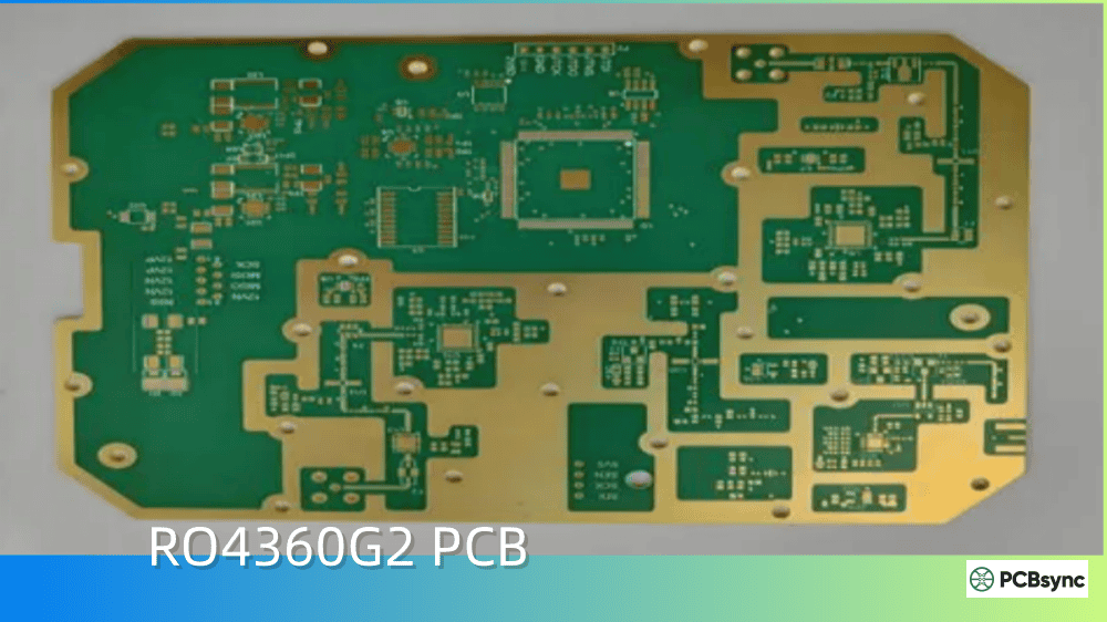
If you’ve been searching for a high-Dk laminate that doesn’t require specialized PTFE processing, RO4360G2 PCB is probably on your shortlist. I’ve worked with this material on several RF designs over the past few years, and honestly, it fills a gap that many engineers didn’t realize existed until Rogers introduced it.
This guide covers everything you need to know about RO4360G2 PCB—from specifications and real-world applications to design considerations and how it compares to other materials in the RO4000 family. Whether you’re designing power amplifiers, patch antennas, or ground-based radar systems, this material deserves a serious look.
RO4360G2 is a glass-reinforced, hydrocarbon ceramic-filled thermoset laminate developed by Rogers Corporation. It belongs to the RO4000 series, which has earned a solid reputation among RF engineers for balancing performance with manufacturability.
What makes RO4360G2 PCB stand out is its dielectric constant (Dk) of 6.15—significantly higher than most other thermoset laminates in its class. This high Dk value allows you to shrink circuit dimensions considerably, which matters when board real estate is at a premium or when you’re trying to hit specific cost targets.
The material was designed from the ground up to process like FR-4. That’s not marketing fluff—it genuinely uses standard epoxy/glass fabrication methods, which means your existing PCB supplier can probably work with it without major equipment changes or learning curves.
Key Characteristics of RO4360G2 PCB
Here’s what you’re getting with this material:
High dielectric constant (Dk = 6.15) for circuit miniaturization
Low loss tangent (Df = 0.0038 at 10 GHz) for minimal signal attenuation
FR-4-like processing without specialized PTFE handling
Lead-free solder compatible for RoHS compliance
CAF resistant for long-term reliability
Compatible with RO4400 series prepreg for multilayer designs
RO4360G2 PCB Technical Specifications
Before diving into design, you need to understand what you’re working with. Here’s the complete specification breakdown based on Rogers’ published data.
A quick note on Design Dk: Rogers recommends using 6.4 for your simulations rather than the process value of 6.15. This accounts for manufacturing tolerances and gives you more realistic results. I’ve learned this the hard way—design to the process Dk and you’ll be chasing impedance issues during prototyping.
The low Z-axis CTE is particularly important for plated through-hole reliability. If you’re building multilayer boards with substantial thermal cycling, this number matters more than most engineers realize.
Mechanical Properties of RO4360G2 PCB
Property
Value
Tensile Modulus (X-axis)
19,000 MPa
Tensile Modulus (Y-axis)
15,000 MPa
Flexural Strength
207 MPa
Peel Strength (1 oz copper)
1.05 N/mm
Moisture Absorption
0.06%
Available Thicknesses and Panel Sizes
RO4360G2 PCB is available in several standard configurations:
Dielectric Thickness
Copper Cladding Options
8 mil (0.203 mm)
½ oz, 1 oz, 2 oz
12 mil (0.305 mm)
½ oz, 1 oz, 2 oz
16 mil (0.406 mm)
½ oz, 1 oz, 2 oz
20 mil (0.508 mm)
½ oz, 1 oz, 2 oz
32 mil (0.813 mm)
½ oz, 1 oz, 2 oz
60 mil (1.524 mm)
½ oz, 1 oz, 2 oz
Standard panel sizes are 12″ × 18″ and 18″ × 24″, though availability can vary by region. Check with your supplier on current stock.
Why Choose RO4360G2 PCB for High-Frequency Designs?
After working with various Rogers materials, I can tell you that RO4360G2 PCB hits a sweet spot for certain applications. Here’s why it deserves consideration:
Circuit Miniaturization with High Dk
The primary advantage of RO4360G2 PCB is its Dk of 6.15—one of the highest available in a thermoset laminate. Higher Dk means shorter wavelengths at a given frequency, which translates directly to smaller circuit dimensions.
For patch antenna designs, this can mean 25-30% size reduction compared to materials with Dk around 3.5. In space-constrained applications like small cell transceivers or compact radar modules, that kind of reduction is significant.
Cost-Effective Alternative to PTFE
Traditional high-Dk materials typically use PTFE (Teflon) substrates, which require specialized fabrication processes. PTFE is notoriously difficult to plate, etch, and handle during lamination. The result? Higher fabrication costs and longer lead times.
RO4360G2 PCB eliminates those headaches. It processes using standard FR-4 methods, which means:
Standard drilling and routing
Conventional oxide treatments for multilayer bonding
No special via preparation needed
Compatible with automated assembly equipment
The total PCB cost savings compared to PTFE alternatives can be substantial, especially in volume production.
Reliable Plated Through-Hole Performance
The low Z-axis CTE (50 ppm/°C) combined with high Tg (>280°C) makes RO4360G2 PCB excellent for PTH reliability. This matters for:
Products requiring multiple reflow cycles
Applications with significant thermal cycling
Designs using heavy copper weights
Lead-free assembly processes
Lead-Free Process Compatibility
RO4360G2 PCB handles lead-free soldering without issues. Peak reflow temperatures up to 260°C are within its capability, making it compliant with RoHS and WEEE requirements without special handling.
RO4360G2 PCB Applications
Based on Rogers’ documentation and real-world implementations, RO4360G2 PCB performs well in these applications:
Base Station Power Amplifiers
Power amplifiers in cellular base stations need materials that can handle heat while maintaining consistent electrical properties. RO4360G2 PCB’s thermal conductivity (0.8 W/m/K) and stable Dk make it a practical choice for PA designs in 4G and 5G infrastructure.
Patch Antennas and Antenna Arrays
The high Dk value is particularly valuable for patch antenna designs where size matters. Smaller patches mean tighter arrays and more compact form factors—essential for modern wireless systems.
Ground-Based Radar Systems
Radar applications demand consistent performance across temperature extremes and long operational lifetimes. The CAF resistance and low moisture absorption of RO4360G2 PCB contribute to reliability in these demanding environments.
Small Cell Transceivers
5G densification relies heavily on small cells. RO4360G2 PCB enables the compact RF front-ends these systems require while keeping costs manageable for high-volume deployment.
General RF and Microwave Circuits
Beyond specific applications, RO4360G2 PCB works well for filters, couplers, combiners, and other RF components where a balance of performance and processability is needed.
Automotive Radar Systems (ADAS)
Modern vehicles increasingly rely on radar for advanced driver assistance systems. Whether it’s adaptive cruise control, collision avoidance, or blind spot detection, these systems require reliable RF performance in harsh automotive environments. RO4360G2 PCB’s temperature stability (-55°C to +125°C operating range) and CAF resistance make it suitable for underhood and exterior automotive applications.
Satellite Communication Systems
Satellite uplink and downlink equipment demands consistent electrical performance despite temperature extremes and radiation exposure. RO4360G2 PCB’s stable dielectric properties and low moisture absorption (0.06%) contribute to long-term reliability in space-adjacent ground equipment and terminal designs.
RO4360G2 PCB vs Other Rogers Materials
Choosing between Rogers PCB materials often comes down to your specific Dk requirements, loss budget, and cost constraints. Here’s how RO4360G2 compares to its siblings.
RO4350B is probably the most widely used material in the RO4000 family. If you don’t specifically need the size reduction from high Dk, RO4350B offers slightly lower loss and better Z-axis CTE.
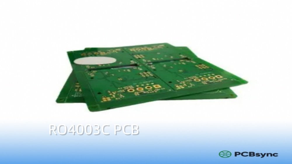
RO4003C has the lowest loss tangent in the RO4000 family and is halogen-free. Choose it when loss is your primary concern and board size isn’t critical.
RO4360G2 vs RO4730G3 Comparison
Parameter
RO4360G2
RO4730G3
Dielectric Constant (Dk)
6.15
3.0
Dissipation Factor (Df)
0.0038
0.0028
Thermal Conductivity
0.8 W/m/K
0.6 W/m/K
Best For
High Dk needs
Lower Dk applications
RO4730G3 is essentially the opposite approach—lower Dk with excellent loss characteristics. The two materials complement each other in hybrid stackups.
RO4360G2 PCB Design Guidelines
Getting the most out of RO4360G2 PCB requires attention to a few key design considerations.
Impedance Control and Trace Calculations
Always use the Design Dk of 6.4 for impedance calculations, not the process value of 6.15. This provides margin for manufacturing variations and gives more accurate first-pass results.
For a 50Ω microstrip line on 20 mil RO4360G2:
Trace width will be narrower than on lower-Dk materials
Edge-coupled lines will have tighter spacing requirements
Verify calculations with your fab house’s DFM tools
Multilayer Stackup Recommendations
RO4360G2 PCB pairs well with RO4400 series prepregs (RO4450F and RO4460G2) for multilayer constructions. You can also combine it with lower-Dk RO4000 laminates like RO4350B or RO4003C in hybrid stackups.
A typical 4-layer stackup might look like:
Layer
Material
Thickness
L1 (Signal)
RO4360G2
20 mil
Prepreg
RO4450F
4 mil
L2 (Ground)
Copper
1 oz
Core
RO4003C
20 mil
L3 (Power)
Copper
1 oz
Prepreg
RO4450F
4 mil
L4 (Signal)
RO4360G2
20 mil
Fabrication Considerations
Desmear: Multilayer constructions require desmear. Both CF4/O2 plasma and alkaline permanganate processes work well.
Oxide Treatment: Standard reduced oxide, brown oxide, or oxide alternatives are compatible.
Lamination: Follow RO4450F processing guidelines for temperature ramps and pressure settings.
Drilling: Standard carbide drills work fine; no special tooling required.
Thermal Management
While RO4360G2 has reasonable thermal conductivity at 0.8 W/m/K, high-power designs may still need thermal vias to ground planes. Plan your via placement during initial layout, not as an afterthought.
Surface Finish Selection for RO4360G2 PCB
The choice of surface finish affects both RF performance and assembly reliability. Common options include:
For RF applications, immersion silver typically offers the best combination of low loss and good solderability. ENIG is preferred when wire bonding or multiple reflow cycles are required.
Copper Weight Considerations
RO4360G2 PCB is available with copper weights from ½ oz to 2 oz. For power amplifier applications, heavier copper (1 oz or 2 oz) improves thermal dissipation and reduces conductor losses. However, heavier copper requires wider trace-to-trace spacing and affects impedance calculations.
Copper Weight
Typical Use Case
½ oz (18 μm)
Low-power RF, fine-pitch designs
1 oz (35 μm)
General purpose, moderate power
2 oz (70 μm)
Power amplifiers, high-current paths
Useful Resources for RO4360G2 PCB Design
Here are the essential documents and tools for working with RO4360G2:
Official Rogers Documentation
RO4360G2 Data Sheet – Complete specifications and typical properties
Laminate Properties Tool – Compare materials and filter by parameters
Access: Rogers ACS website
Material Availability
Contact Rogers regional sales for current availability
Standard lead times vary; check with your PCB supplier
Regional finished goods inventory helps reduce lead times
Frequently Asked Questions About RO4360G2 PCB
What is the dielectric constant of RO4360G2?
RO4360G2 has a process dielectric constant (Dk) of 6.15 ± 0.15 measured at 10 GHz and 23°C. For circuit design and simulation purposes, Rogers recommends using a Design Dk of 6.4, which accounts for manufacturing variations and provides more accurate impedance predictions.
Is RO4360G2 PCB compatible with lead-free soldering?
Yes, RO4360G2 PCB is fully compatible with lead-free assembly processes. The material can withstand peak reflow temperatures required for lead-free solders (typically up to 260°C) without degradation. This makes it compliant with RoHS and WEEE directives.
Can RO4360G2 be processed like standard FR-4?
Absolutely—this is one of the material’s key advantages. RO4360G2 uses standard epoxy/glass fabrication processes including conventional drilling, routing, plating, and lamination. No specialized PTFE handling procedures are required, which simplifies manufacturing and reduces costs.
What prepreg should I use with RO4360G2 in multilayer PCBs?
Rogers recommends pairing RO4360G2 with RO4400 series bondplys (RO4450F or RO4460G2) for multilayer constructions. These prepregs are compatible with the lamination temperatures used for RO4360G2 and provide good adhesion and flow characteristics. You can also combine RO4360G2 with lower-Dk RO4000 laminates in hybrid stackups.
How does RO4360G2 compare to PTFE materials in terms of cost?
RO4360G2 PCB offers significant cost savings compared to PTFE-based high-Dk materials. The savings come from multiple factors: lower raw material cost, FR-4-like processing (no specialized fabrication), better yields due to easier handling, and compatibility with standard assembly equipment. Total PCB cost reductions of 20-40% compared to PTFE alternatives are common, depending on design complexity.
Final Thoughts on RO4360G2 PCB
RO4360G2 PCB represents a practical solution for engineers who need high dielectric constant performance without the complexity and cost of PTFE materials. Its combination of a Dk of 6.15, low loss, and FR-4-like processing makes it valuable for size-constrained RF applications.
The material excels in power amplifier designs, patch antennas, radar systems, and small cell transceivers—anywhere that circuit miniaturization matters and fabrication simplicity is valued.
If you’re considering RO4360G2 for your next design, start with the official Rogers datasheet, run your impedance calculations using the Design Dk of 6.4, and confirm material availability with your PCB supplier. The combination of performance and processability makes it worth the evaluation effort.
Inquire: Call 0086-755-23203480, or reach out via the form below/your sales contact to discuss our design, manufacturing, and assembly capabilities.
Quote: Email your PCB files to Sales@pcbsync.com (Preferred for large files) or submit online. We will contact you promptly. Please ensure your email is correct.
Notes: For PCB fabrication, we require PCB design file in Gerber RS-274X format (most preferred), *.PCB/DDB (Protel, inform your program version) format or *.BRD (Eagle) format. For PCB assembly, we require PCB design file in above mentioned format, drilling file and BOM. Click to download BOM template To avoid file missing, please include all files into one folder and compress it into .zip or .rar format.


