Inquire: Call 0086-755-23203480, or reach out via the form below/your sales contact to discuss our design, manufacturing, and assembly capabilities.
Quote: Email your PCB files to Sales@pcbsync.com (Preferred for large files) or submit online. We will contact you promptly. Please ensure your email is correct.
Notes: For PCB fabrication, we require PCB design file in Gerber RS-274X format (most preferred), *.PCB/DDB (Protel, inform your program version) format or *.BRD (Eagle) format. For PCB assembly, we require PCB design file in above mentioned format, drilling file and BOM. Click to download BOM template To avoid file missing, please include all files into one folder and compress it into .zip or .rar format.
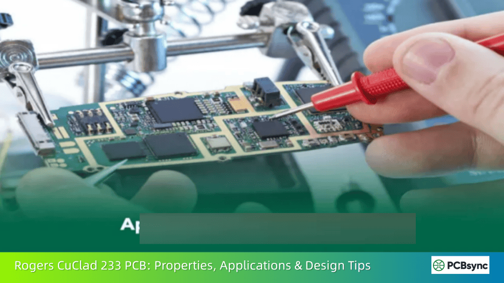
If you’ve ever worked on RF or microwave circuit design, you know how critical material selection is. One wrong choice, and your carefully designed filter or LNA starts behaving like a different circuit entirely at high frequencies. That’s whereCuClad 233comes in—a PTFE-based laminate from Rogers Corporation that’s become a go-to substrate for engineers working on demanding high-frequency applications.
I’ve spent years specifying PCB materials for various RF projects, and CuClad 233 consistently delivers where it matters: predictable electrical performance, reasonable fabrication characteristics, and that crucial balance between cost and capability.
CuClad 233 is a woven fiberglass-reinforced PTFE (polytetrafluoroethylene) composite laminate manufactured by Rogers Corporation. The “233” designation refers to its nominal dielectric constant of 2.33, which places it in the sweet spot for many RF and microwave applications.
What sets CuClad 233 apart from other PTFE laminates is its cross-plied construction. The alternating glass fiber plies are oriented at 90° to each other, providing true electrical and mechanical isotropy in the X-Y plane. This is something you won’t find in many competing materials, and it matters significantly when you’re designing phased array antennas or other applications where consistent behavior across different orientations is essential.
The material uses a medium fiberglass-to-PTFE ratio, which Rogers engineered to strike a balance: you get a lower dielectric constant and improved dissipation factor without sacrificing the mechanical properties that make fabrication practical.
Key Properties and Specifications of CuClad 233
Understanding the technical specifications of CuClad 233 is essential for proper design integration. Here’s what you need to know:
The low dissipation factor of 0.0013 at 10 GHz is particularly noteworthy. This translates directly to reduced signal loss in your circuits—critical when you’re designing anything that operates in the X-band or above.
Why Engineers Choose CuClad 233: Key Benefits
Low Dielectric Constant for Better Performance
The Dk of 2.33 enables wider trace widths for a given impedance target. This isn’t just convenient—it directly impacts your yield rates and manufacturing costs. Wider traces mean better etching tolerances and reduced sensitivity to fabrication variations.
Excellent Dimensional Stability
The cross-plied woven glass construction provides significantly better dimensional stability compared to non-woven PTFE composites. When you’re designing multilayer boards or need tight registration between layers, this stability becomes essential.
CTE Matching with Aluminum
Here’s something many engineers overlook: the in-plane CTE of CuClad 233 closely matches aluminum. If you’re designing antenna systems that mount directly to aluminum aircraft skins or structures, this reduces thermal stress at the interface—a real consideration for aerospace applications.
Low Moisture Absorption
At 0.02% water absorption, CuClad 233 maintains its electrical properties even in humid environments. The low outgassing characteristics also make it suitable for certain space-adjacent applications where contamination is a concern.
Consistent Performance Across Frequency
The stable Dk over a wide frequency range means your impedance calculations remain valid as you move through different operating bands. This predictability simplifies the design process and reduces the need for empirical tuning.
CuClad 233 Applications in Industry
Military Radar and Electronic Warfare
CuClad 233 has established itself in defense applications, particularly in radar systems, electronic countermeasures (ECM), and electronic support measures (ESM). The material’s combination of low loss, dimensional stability, and reliable performance under varying environmental conditions makes it well-suited for military-grade equipment.
Phased Array Antenna Systems
The true isotropy in the X-Y plane is crucial for phased array applications. When you’re dealing with hundreds or thousands of antenna elements that need to behave identically regardless of their orientation, material consistency becomes non-negotiable. CuClad 233’s cross-plied construction delivers this consistency.
Microwave Components
Low-noise amplifiers (LNAs), filters, and couplers frequently specify CuClad 233 as the substrate material. These components demand:
Predictable dielectric constant for accurate impedance matching
Low loss to preserve signal integrity
Stable performance across temperature variations
Satellite and Space Communications
For satellite communication systems operating in C-band and above, the low moisture absorption and stable electrical properties make CuClad 233 a practical choice. The material can handle the thermal cycling associated with space-adjacent environments.
5G Infrastructure
As 5G networks push into higher frequency bands, the demand for low-loss substrates continues to grow. CuClad 233’s performance characteristics align well with the requirements of 5G antenna systems and millimeter-wave circuits.
Better dimensional stability than non-woven alternatives
A balance between electrical performance and processability
Compatibility with aluminum structures (CTE matching)
Consider alternatives when:
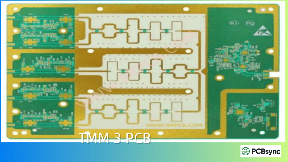
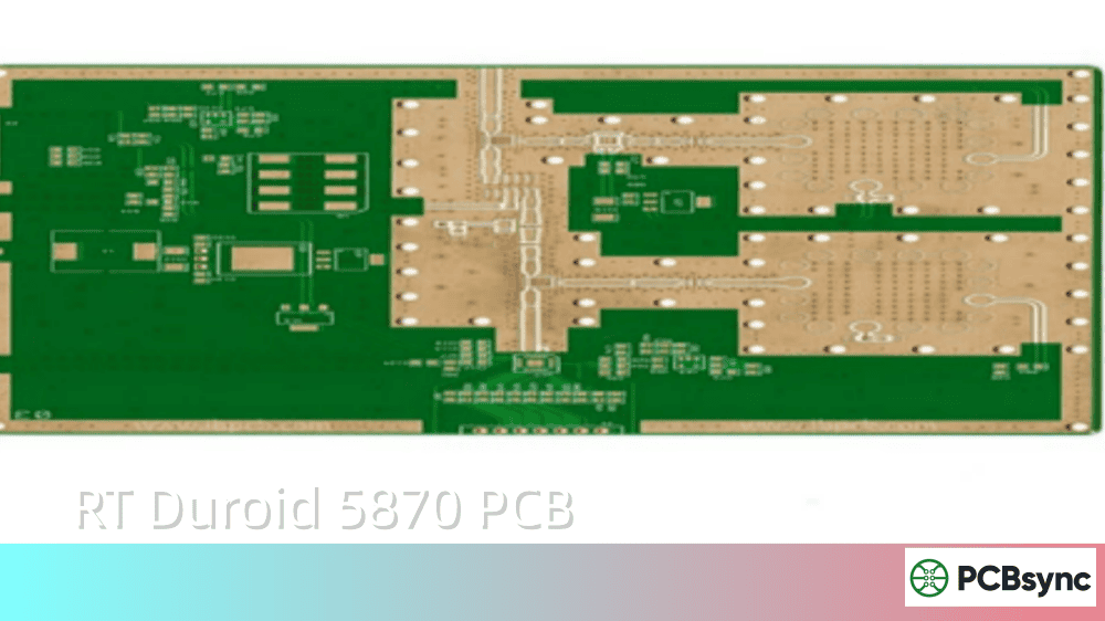
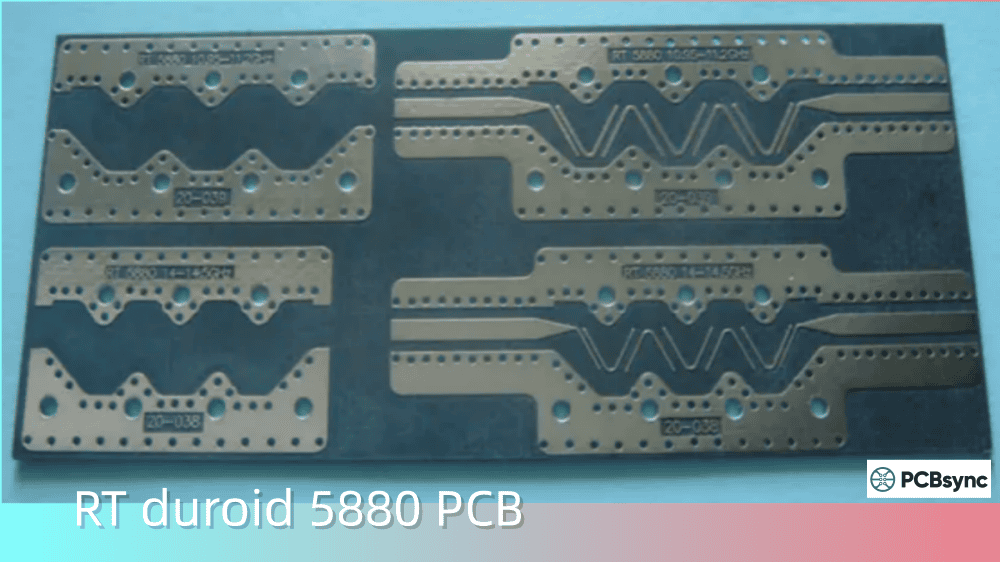
Absolute lowest loss is critical (CuClad 217 or RT/duroid 5880)
Processing cost is the primary driver (RO4003C)
Higher mechanical strength is required (CuClad 250)
Design Tips for CuClad 233 PCBs
Impedance Control Considerations
When designing with CuClad 233, use the design Dk value of 2.40 for impedance calculations rather than the process Dk of 2.33. This accounts for the glass weave effect and provides more realistic predictions for your actual circuit performance.
Verify with your fabricator’s impedance modeling tools
Request test coupons for critical applications
Stackup Design
CuClad 233 works well in both single-layer and multilayer constructions. For hybrid stackups combining CuClad 233 with FR-4 or other materials:
Match CTE values where possible to minimize warpage
Consider using Rogers CuClad 6250 or 6700 bonding films for multilayer PTFE constructions
Position the CuClad 233 layer at the critical RF interfaces
Trace Width and Spacing
The low Dk of 2.33 allows for wider traces at standard impedances:
Impedance Target
Approximate Trace Width (10 mil substrate)
50 Ω microstrip
~25 mils
75 Ω microstrip
~12 mils
These wider traces improve manufacturing yield and reduce sensitivity to etching variations.
Thermal Management
While CuClad 233’s thermal conductivity (0.26 W/m/K) is adequate for most applications, high-power designs may require additional thermal management. Consider:
Metal backing (aluminum, brass, or copper plates)
Thermal vias in ground planes
Heat spreader integration
Fabrication Guidelines for CuClad 233
Drilling Considerations
PTFE-based laminates like CuClad 233 require attention during drilling:
Use sharp carbide drill bits with 130° point geometry
Reduce surface speed to prevent PTFE smearing (100 SFM or less recommended)
Use hard phenolic entry material (10–25 mil) to clean debris from drill bits
Implement peck drilling for high aspect ratio holes to prevent bird-nesting
Plated Through-Hole Preparation
The PTFE surface requires treatment before electroless copper plating:
Sodium naphthalene etch is the traditional approach—effective but requires careful handling
Plasma treatment using hydrogen/nitrogen gas mixtures (30–70% H₂, 70–30% N₂) is an alternative
Both methods prepare the PTFE surface for reliable copper adhesion.
Lamination Process
For multilayer boards:
Clean surfaces thoroughly before lamination (chemical cleaning preferred over mechanical scrubbing)
Use vacuum lamination at 370–390°F (190–200°C) under 200–300 psi
Implement gradual ramp-up and cool-down to avoid trapped air and warpage
Solder Mask Application
Apply solder mask within 12 hours of etching. For improved adhesion:
Process through a sodium etch cycle or plasma treatment
Pre-bake to remove residual moisture from the laminate
Available Configurations and Ordering
CuClad 233 is available in the following standard configurations:
Copper Cladding Options
½ oz (17.5 µm)
1 oz (35 µm)
2 oz (70 µm) electrodeposited copper
Rolled copper foil is available for applications requiring reduced surface roughness.
Panel Sizes
Maximum available size: 36″ × 48″ (914 mm × 1219 mm)
Thickness Options
Multiple dielectric thicknesses are available. Contact Rogers Corporation or authorized distributors for specific thickness availability.
Special Testing
For critical applications, specify “LX” testing grade. This ensures each sheet is individually tested with a test report included with the order.
Is CuClad 233 compatible with lead-free soldering processes?
Yes. CuClad 233 is fully compatible with lead-free assembly processes. The material maintains its structural integrity through the higher temperatures required for lead-free reflow (typically 260°C peak).
What frequency range is CuClad 233 suitable for?
CuClad 233 performs well from DC through millimeter-wave frequencies. The stable dielectric constant and low loss tangent make it suitable for applications up to 30 GHz and beyond, depending on circuit design and manufacturing precision.
How does CuClad 233 compare to FR-4 for high-frequency applications?
FR-4 is inadequate for most high-frequency applications above a few GHz. Compared to FR-4, CuClad 233 offers significantly lower dielectric loss (0.0013 vs. ~0.020), more stable Dk with frequency and temperature, and better controlled electrical properties. The tradeoff is higher material cost and more specialized fabrication requirements.
Can CuClad 233 be used in hybrid constructions with FR-4?
Yes, hybrid stackups are common. Position the CuClad 233 at the critical RF layers (typically outer layers for microstrip designs) while using FR-4 for inner layers where high-frequency performance isn’t required. Pay attention to CTE differences during lamination to prevent warpage.
What’s the difference between CuClad 233 and DiClad 870?
Both have similar Dk values (~2.33), but CuClad 233 features cross-plied construction while DiClad 870 uses aligned plies. The cross-plied construction of CuClad 233 provides true isotropy in the X-Y plane, making it better suited for phased array antennas and applications requiring consistent performance regardless of trace orientation.
Simulation and Modeling Considerations
When designing circuits on CuClad 233, proper material characterization in your simulation tools is essential. Most commercial EM simulators support Rogers materials natively:
Ansys HFSS and SIwave — 3D planar EM simulation for signal integrity and EMI analysis up to 40+ GHz
Keysight ADS — Integrated 2D/3D EM simulation with circuit co-simulation
Cadence Allegro — Signal integrity analysis with controlled impedance support
When setting up simulations, always use Rogers’ published data for the operating frequency range. The design Dk value (2.40) accounts for manufacturing tolerances and glass weave effects that purely theoretical calculations might miss.
For critical applications, request material characterization data from Rogers or perform your own measurements using resonant cavity or transmission line methods.
Final Thoughts
CuClad 233 remains a solid choice for RF and microwave applications that demand consistent electrical performance without the extreme cost of pure PTFE laminates. Its cross-plied construction, stable dielectric properties, and reasonable fabrication characteristics make it particularly valuable for antenna systems, military electronics, and communication equipment.
The key to success with CuClad 233—like any high-frequency material—lies in understanding its properties and designing accordingly. Use the design Dk value for impedance calculations, work with a fabricator experienced in PTFE processing, and don’t underestimate the importance of proper hole preparation and surface treatment.
For engineers working on critical RF applications, CuClad 233 provides the predictable foundation your designs need to perform as intended when they leave the simulation environment and enter the real world.
Inquire: Call 0086-755-23203480, or reach out via the form below/your sales contact to discuss our design, manufacturing, and assembly capabilities.
Quote: Email your PCB files to Sales@pcbsync.com (Preferred for large files) or submit online. We will contact you promptly. Please ensure your email is correct.
Notes: For PCB fabrication, we require PCB design file in Gerber RS-274X format (most preferred), *.PCB/DDB (Protel, inform your program version) format or *.BRD (Eagle) format. For PCB assembly, we require PCB design file in above mentioned format, drilling file and BOM. Click to download BOM template To avoid file missing, please include all files into one folder and compress it into .zip or .rar format.


