Inquire: Call 0086-755-23203480, or reach out via the form below/your sales contact to discuss our design, manufacturing, and assembly capabilities.
Quote: Email your PCB files to Sales@pcbsync.com (Preferred for large files) or submit online. We will contact you promptly. Please ensure your email is correct.
Notes: For PCB fabrication, we require PCB design file in Gerber RS-274X format (most preferred), *.PCB/DDB (Protel, inform your program version) format or *.BRD (Eagle) format. For PCB assembly, we require PCB design file in above mentioned format, drilling file and BOM. Click to download BOM template To avoid file missing, please include all files into one folder and compress it into .zip or .rar format.
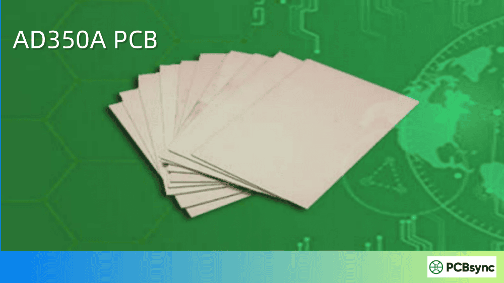
If you’ve been searching for a high-frequency PCB material that handles serious thermal demands without compromising on RF performance, you’ve probably come across the AD350A. I’ve worked with this material on several antenna and power amplifier projects over the past few years, and it’s become my go-to choice for applications where heat dissipation is as critical as electrical performance.
In this guide, I’ll walk you through everything you need to know about the AD350A laminate—from its core specifications to real-world design considerations. Whether you’re evaluating materials for a 5G base station antenna or a satellite communication system, this article covers the technical details that actually matter.
The AD350A is a specialty laminate developed by Rogers Corporation (originally under the Arlon brand before acquisition). It belongs to the AD Series of antenna-grade materials specifically engineered for high-frequency PCB applications.
At its core, the AD350A combines three key components:
PTFE (Polytetrafluoroethylene) – The fluoropolymer resin base provides excellent dielectric properties
Ceramic filler – Enhances thermal conductivity and controls the dielectric constant
This combination creates a material with a unique balance: the low-loss characteristics of PTFE-based laminates, the processability benefits of woven glass reinforcement, and superior thermal management from ceramic loading.
The AD350A was specifically redeveloped from the original AD350 formulation to deliver higher thermal conductivity, lower thermal expansion, and improved copper bond integrity. That “A” designation matters—it represents measurable improvements in real-world performance.
AD350A Key Properties and Specifications
Let me break down the critical specifications that define the AD350A’s performance. These numbers come directly from Rogers’ official datasheet and represent the values you’ll need for your design calculations.
The design Dk of 3.50 ± 0.05 is particularly noteworthy. This tight tolerance means your impedance calculations will be consistent from board to board—critical for antenna designs where even small Dk variations can shift resonant frequencies.
Thermal and Mechanical Properties
Property
Typical Value
Test Method
Thermal Conductivity
0.45 W/m-K (Z-axis)
–
CTE (X-axis)
11 ppm/°C
ASTM D3386-00
CTE (Y-axis)
14 ppm/°C
ASTM D3386-00
CTE (Z-axis)
35 ppm/°C
IPC TM-650 2.4.41
Moisture Absorption
0.01% – 0.2%
–
Copper Peel Strength
>6 lb/in (typical)
IPC TM-650 2.4.8
Flexural Strength
15,000+ psi
ASTM D790
That 0.45 W/m-K thermal conductivity in the Z-axis is what sets the AD350A apart from standard PTFE laminates. It’s roughly 50% higher than many competing materials in the same Dk range, which translates directly to better heat dissipation in power amplifier applications.
Available Configurations
The AD350A is available in several configurations to suit different design requirements:
Configuration
Details
Standard Thicknesses
0.010″ to 0.125″
Copper Cladding
0.5 oz to 2 oz (ED and rolled copper)
Panel Sizes
36″ × 48″ and 36″ × 72″
Special Options
Heavy metal ground planes (aluminum, brass, copper)
The heavy metal backing option is worth noting—having an integral aluminum or copper heat sink bonded directly to the AD350A substrate simplifies thermal management in high-power designs.
Why Choose AD350A? Key Advantages
After working with multiple high-frequency materials, here’s why the AD350A often wins the selection process for certain applications:
1. Superior Thermal Performance
The combination of high thermal conductivity (0.45 W/m-K) and low Z-axis CTE (35 ppm/°C) makes the AD350A ideal for designs where temperature extremes are normal. Power amplifiers running at elevated temperatures maintain consistent performance because the material efficiently moves heat away from active components.
2. Excellent Dk Stability
The ± 0.05 tolerance on dielectric constant is tighter than many PTFE competitors. This translates to more predictable antenna patterns and filter responses. When you’re designing a phased array where element-to-element consistency matters, that Dk tolerance becomes critical.
3. Low PIM for Antenna Applications
PIM values of -159 to -163 dBc make the AD350A suitable for base station antennas and other applications where passive intermodulation must be minimized. High PIM can create interference that degrades system sensitivity—not something you want in a 5G deployment.
4. Standard PTFE Processing Compatibility
Unlike some exotic materials, the AD350A works with established PTFE fabrication processes. Your PCB manufacturer doesn’t need new equipment or specialized training. This compatibility keeps costs reasonable and lead times predictable.
5. Improved PTH Reliability
The lower Z-axis CTE compared to traditional PTFE laminates (35 ppm/°C vs. 50+ ppm/°C) improves plated through-hole reliability during thermal cycling. Fewer barrel cracks mean better long-term reliability in field-deployed systems.
The AD350A’s thermal and electrical properties make it suitable for several demanding application areas:
Telecommunications Infrastructure
Base station antennas for 4G LTE and 5G networks rely heavily on materials like the AD350A. The low PIM ensures clean signal transmission, while thermal stability maintains antenna patterns under varying environmental conditions. Multi-band antennas particularly benefit from the consistent Dk across temperature ranges.
Aerospace and Defense
Military radar systems, satellite communication terminals, and aircraft-mounted antennas face extreme temperature swings. The AD350A’s thermal performance and dimensional stability make it a trusted choice for these mission-critical applications. Electronic warfare systems and surveillance equipment also utilize this material.
Power Amplifiers
High-power RF amplifiers generate significant heat. The AD350A’s thermal conductivity helps manage junction temperatures, improving device reliability and potentially allowing higher output power from the same footprint. Gallium nitride (GaN) power amplifier modules particularly benefit from improved thermal dissipation.
Automotive Radar
Advanced driver assistance systems (ADAS) use 77 GHz radar modules that must perform reliably across automotive temperature ranges (-40°C to +125°C). The AD350A’s low TCDk keeps radar accuracy consistent regardless of under-hood temperatures.
Carrier-Grade Wi-Fi
Enterprise Wi-Fi access points and outdoor wireless backhaul equipment benefit from the AD350A’s combination of RF performance and environmental resilience.
AD350A vs. Other High-Frequency Laminates
Choosing the right material often comes down to comparing alternatives. Here’s how the AD350A stacks up against common competitors:
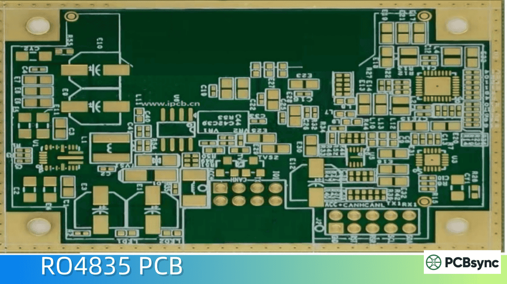
AD350A vs. RO4350B
Parameter
AD350A
RO4350B
Material Type
PTFE/Ceramic/Woven Glass
Hydrocarbon/Ceramic/Woven Glass
Dielectric Constant (Dk)
3.50 ± 0.05
3.48 ± 0.05
Dissipation Factor (Df) @ 10 GHz
0.0033
0.0037
Thermal Conductivity (Z-axis)
0.45 W/m-K
0.69 W/m-K
Z-axis CTE
35 ppm/°C
41 ppm/°C
Processing
PTFE processes
FR-4 compatible
UL 94 Rating
V-0 (available)
V-0
Cost
Higher
Moderate
When to choose AD350A: When you need PTFE-based performance with better PIM characteristics, or when your existing supply chain is PTFE-focused.
When to choose RO4350B: When FR-4 processing compatibility is important, or when higher thermal conductivity is the priority. RO4350B is also generally more cost-effective for volume production.
AD350A vs. Standard FR-4
Parameter
AD350A
FR-4
Dielectric Constant (Dk)
3.50
4.2 – 4.8
Dissipation Factor (Df)
0.0033
0.016 – 0.025
Dk Tolerance
± 0.05
± 0.3 (typical)
Max Operating Frequency
40+ GHz
< 1 GHz (practical)
Thermal Conductivity
0.45 W/m-K
0.25 – 0.3 W/m-K
Cost
10-20× higher
Baseline
The AD350A costs significantly more than FR-4, but the performance difference justifies the expense for RF and microwave applications. You simply cannot build a functional 10 GHz circuit on FR-4—the losses would be unacceptable.
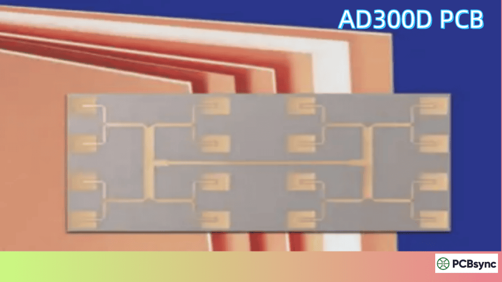
AD350A vs. AD300D
Both materials are part of Rogers’ AD Series, but serve different design needs:
Parameter
AD350A
AD300D
Dielectric Constant (Dk)
3.50
2.94
Dissipation Factor (Df)
0.0033
0.0021
Thermal Conductivity
0.45 W/m-K
Lower
Primary Focus
Thermal performance
Lower Dk, lower loss
Choose AD300D when you need lower Dk for specific antenna designs or when insertion loss is the primary concern. Choose AD350A when thermal management is critical or when the 3.50 Dk fits your design requirements.
PCB Fabrication Guidelines for AD350A
Working with the AD350A requires attention to PTFE-specific fabrication processes. Here are the key considerations:
Drilling
Use carbide drills with appropriate geometries for PTFE materials
Control spindle speeds and feed rates to prevent smearing
Entry and exit materials help produce clean holes
Typical drill speeds: 150-200 SFM (surface feet per minute)
Plated Through-Holes (PTH)
Sodium etch or plasma treatment required for PTFE adhesion
The AD350A’s ceramic loading can affect etchant consumption
Monitor dwell times to achieve proper surface preparation without over-etching
The improved Z-axis CTE (35 ppm/°C) provides better PTH reliability than standard PTFE
Lamination
Compatible with standard PTFE bonding prepregs
Hybrid constructions (AD350A + FR-4) are possible for cost optimization
Control lamination pressure and temperature per Rogers’ recommendations
Available with various copper weights from 0.5 to 2 oz
Material is relatively stable but follow standard laminate handling practices
Shelf life typically 12+ months under proper conditions
Design Tips for AD350A PCBs
From my experience designing with the AD350A, here are practical recommendations:
Impedance Calculations
Use the design Dk value (3.50) rather than the process Dk (3.54) for impedance calculations. The design value accounts for the actual operating conditions your board will see. Most impedance calculators like Saturn PCB Toolkit handle this properly if you input the correct material parameters.
Thermal Via Placement
While the AD350A has good thermal conductivity for a PTFE material, thermal vias still help in high-power designs. Place thermal vias directly under heat-generating components to create low-resistance thermal paths to ground planes or metal backing.
Mixed Dielectric Stackups
For cost optimization, consider hybrid stackups with AD350A used only on RF layers and FR-4 for digital or power distribution layers. This approach captures the RF performance where needed while reducing overall material cost. Work closely with your PCB manufacturer to ensure proper bonding between dissimilar materials.
Design for Manufacturing (DFM)
Keep trace widths above 5 mils where possible for consistent etching
Allow adequate spacing for your operating frequency
Consider the panel sizes (36″ × 48″ or 36″ × 72″) when laying out your design
Communicate early with your fabricator about material availability and lead times
The AD350A has a design dielectric constant (Dk) of 3.50 ± 0.05 at 10 GHz. The process Dk measured under laboratory conditions is 3.54. For impedance calculations and simulation, use the design value of 3.50 as it better represents real-world operating conditions. The tight ± 0.05 tolerance ensures consistent electrical performance from board to board.
Is AD350A compatible with standard FR-4 processing?
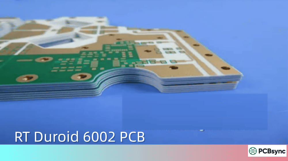
Not entirely. The AD350A uses PTFE-based processing rather than FR-4 processing. It requires sodium etch or plasma treatment for proper PTH adhesion—steps not needed for FR-4. However, if you’re already set up for PTFE fabrication (such as for RT/duroid or other Rogers PTFE materials), the AD350A fits into existing processes. For FR-4 process compatibility, consider Rogers RO4350B instead.
What applications is AD350A best suited for?
The AD350A excels in applications requiring both high-frequency performance and superior thermal management. Primary applications include telecommunications base station antennas, power amplifiers, aerospace and defense radar systems, satellite communication equipment, and automotive radar modules. Its low PIM characteristics make it particularly valuable for antenna applications where passive intermodulation could degrade system performance.
How does AD350A compare to RO4350B?
Both are excellent high-frequency materials but serve different needs. The AD350A is PTFE-based with better PIM performance, while RO4350B is hydrocarbon-based with easier FR-4-style processing. RO4350B has higher thermal conductivity (0.69 W/m-K vs. 0.45 W/m-K). Choose AD350A when PTFE processing compatibility or low PIM is required; choose RO4350B when FR-4 fabrication compatibility and cost are priorities.
What thicknesses are available for AD350A?
The AD350A is available in standard thicknesses ranging from 0.010″ to 0.125″. Copper cladding options include 0.5 oz, 1 oz, and 2 oz in both electrodeposited and rolled copper foils. Standard panel sizes are 36″ × 48″ and 36″ × 72″. The material can also be supplied bonded to heavy metal ground planes (aluminum, brass, or copper) for applications requiring integral heat sinking.
Conclusion
The AD350A occupies a specific niche in the high-frequency PCB material landscape—it’s the choice when thermal performance matters as much as electrical performance. Its combination of controlled Dk, low loss, excellent thermal conductivity, and low PIM makes it a proven solution for demanding antenna and power amplifier applications.
Is it the right material for every RF project? No. For many designs, RO4350B offers better cost-performance with easier processing. But when temperature extremes are part of the operating environment, when PIM specifications are stringent, or when your fabrication partner already runs PTFE processes, the AD350A delivers reliable performance.
If you’re evaluating the AD350A for your next design, request samples from Rogers and work closely with your PCB manufacturer to confirm they have the right processes in place. The material’s specifications are only as good as the fabrication quality—choose partners with proven PTFE experience.
Inquire: Call 0086-755-23203480, or reach out via the form below/your sales contact to discuss our design, manufacturing, and assembly capabilities.
Quote: Email your PCB files to Sales@pcbsync.com (Preferred for large files) or submit online. We will contact you promptly. Please ensure your email is correct.
Notes: For PCB fabrication, we require PCB design file in Gerber RS-274X format (most preferred), *.PCB/DDB (Protel, inform your program version) format or *.BRD (Eagle) format. For PCB assembly, we require PCB design file in above mentioned format, drilling file and BOM. Click to download BOM template To avoid file missing, please include all files into one folder and compress it into .zip or .rar format.


