Inquire: Call 0086-755-23203480, or reach out via the form below/your sales contact to discuss our design, manufacturing, and assembly capabilities.
Quote: Email your PCB files to Sales@pcbsync.com (Preferred for large files) or submit online. We will contact you promptly. Please ensure your email is correct.
Notes: For PCB fabrication, we require PCB design file in Gerber RS-274X format (most preferred), *.PCB/DDB (Protel, inform your program version) format or *.BRD (Eagle) format. For PCB assembly, we require PCB design file in above mentioned format, drilling file and BOM. Click to download BOM template To avoid file missing, please include all files into one folder and compress it into .zip or .rar format.
If you’ve ever designed a circuit board and wondered why the default PCB thickness is always 1.6mm, you’re not alone. After 15 years of designing everything from consumer electronics to aerospace systems, I’ve learned that board thickness is one of those parameters that can make or break your project—yet it’s often treated as an afterthought.
In this guide, I’ll walk you through everything you need to know about PCB thickness: the standards that exist (and why they exist), how to choose the right thickness for your application, and the practical trade-offs you’ll face during manufacturing. Whether you’re working on a wearable device that demands ultra-thin boards or a high-power industrial controller that needs serious mechanical strength, this guide has you covered.
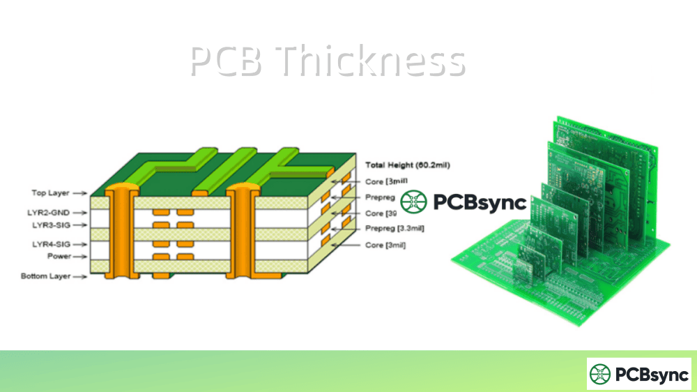
PCB thickness refers to the total vertical measurement of a finished printed circuit board, measured from the top surface to the bottom surface. This measurement includes all the layers that make up your board: the substrate material (typically FR-4), copper layers, prepreg layers in multilayer boards, solder mask, and surface finish.
The overall PCB thickness is determined by the combined thicknesses of several components:
Substrate/Core Material: The insulating base layer (usually FR-4 epoxy-glass laminate)
Copper Layers: The conductive traces and planes
Prepreg Layers: Bonding material between layers in multilayer boards
Solder Mask: Protective coating on outer layers (typically 0.5-1.2 mils)
Surface Finish: HASL, ENIG, OSP, etc. (varies by type)
Understanding this composition is crucial because each element contributes not just to thickness but also to the board’s electrical and mechanical properties.
Standard PCB Thickness Values
While there’s no official industry mandate for PCB thickness, certain values have become de facto standards due to historical reasons and manufacturing optimization.
The 1.6mm Standard: A Brief History
The most common PCB thickness—1.6mm (0.063 inches or 62 mils)—traces back to the early days of circuit board manufacturing. Back then, Bakelite sheets commonly used for electronic substrates came in 1/16-inch thickness, which happens to be approximately 1.57mm. When edge connectors became popular for board-to-board connections, this thickness became the reference standard, and it stuck.
Today, 1.6mm remains the default because manufacturing equipment, component specifications, and connector systems are all optimized around this value. Using it means lower costs and faster turnaround times.
Common PCB Thickness Options
Thickness (mm)
Thickness (inches)
Thickness (mils)
Common Applications
0.2
0.008
8
Ultra-thin flex, wearables
0.4
0.016
16
Flexible PCBs, SIM cards
0.6
0.024
24
Smartphones, tablets
0.8
0.031
31
Compact consumer electronics
1.0
0.039
39
Laptops, thin devices
1.2
0.047
47
General electronics
1.6
0.063
63
Industry standard
2.0
0.079
79
Industrial, automotive
2.4
0.094
94
High-power applications
3.2
0.125
125
Heavy-duty, backplanes
PCB Thickness by Layer Count
The number of layers significantly impacts overall board thickness. Here’s what you can typically expect:
Layer Count
Typical Thickness Range
Standard Thickness
1-2 Layers
0.4mm – 1.6mm
1.6mm
4 Layers
0.8mm – 1.6mm
1.6mm
6 Layers
1.0mm – 2.0mm
1.6mm
8 Layers
1.2mm – 2.4mm
1.6mm – 2.0mm
10+ Layers
1.6mm – 3.2mm+
Varies by design
For boards with 6 or fewer layers, manufacturers can typically achieve the standard 1.6mm thickness. Once you exceed 8 layers, maintaining that thickness requires thinner dielectric layers, which can increase costs and affect impedance control.
Factors That Affect PCB Thickness Selection
Choosing the right PCB thickness isn’t arbitrary—it requires balancing multiple technical and practical considerations.
Layer Count and Stackup Design
Every additional layer adds to your overall thickness. A typical internal copper layer adds about 35µm (1oz copper), while prepreg layers between them add 50-100µm depending on the type. If you’re designing a 12-layer board and need to hit a specific thickness target, you may need to use thinner prepregs or specify reduced copper weights on internal layers.
Pro tip: Always work with your fabricator early in the design process to establish a realistic stackup. They’ll have specific core and prepreg materials in stock, and building around their standard offerings saves money and lead time.
Prepreg Types and Thickness
Prepreg (pre-impregnated) material bonds the layers in multilayer PCBs. Understanding prepreg options helps you achieve precise thickness targets and impedance values.
Common Prepreg Designations:
Prepreg Type
Nominal Thickness
Typical Use
106
0.05mm (2 mils)
Thin dielectric, impedance control
1080
0.076mm (3 mils)
Standard, good resin content
2113
0.1mm (4 mils)
Medium thickness
2116
0.12mm (4.7 mils)
Standard multilayer construction
7628
0.18mm (7 mils)
Thick dielectric, mechanical strength
The actual thickness after lamination depends on the copper pattern beneath—areas with more copper coverage result in thinner dielectric than areas with less coverage. This “resin flow” effect must be accounted for in impedance calculations, which is why working with your fabricator’s specific materials and providing accurate copper coverage data yields the best results.
Copper Weight and Thickness
Copper thickness is specified in ounces per square foot (oz/ft²), where 1oz equals approximately 35µm or 1.37 mils. Standard options include:
Copper Weight
Thickness (µm)
Thickness (mils)
Typical Use
0.5 oz
17.5
0.7
HDI, fine traces
1 oz
35
1.4
General purpose (default)
2 oz
70
2.8
Power circuits
3 oz
105
4.1
High-current applications
4 oz
140
5.5
Heavy power, busbars
If your design requires 2oz or 3oz copper for power handling, factor this into your overall thickness calculations. Heavier copper also affects minimum trace width and spacing requirements.
A common mistake I see is specifying heavy copper without considering the manufacturing implications. With 2oz copper, your minimum trace width typically increases to 8-10 mils (versus 4-5 mils for 1oz), and etching becomes more challenging. Some designs use mixed copper weights—heavier copper on power layers and standard 1oz on signal layers—to balance current capacity with routing density.
Substrate Material Selection
The substrate or core material forms the foundation of your PCB and significantly impacts both thickness options and electrical performance. FR-4 remains the most common choice, but other materials serve specific needs:
Material selection affects available thickness options because manufacturers stock specific laminate thicknesses. Standard FR-4 cores come in thicknesses like 0.1mm, 0.2mm, 0.3mm, 0.4mm, 0.5mm, 0.7mm, 1.0mm, and 1.5mm. High-frequency laminates may have different standard offerings, so verify availability before finalizing your stackup.
Signal Type and Impedance Requirements
For high-speed digital and RF designs, PCB thickness directly impacts controlled impedance. The characteristic impedance of a trace depends on:
Trace width and thickness
Distance to reference plane (dielectric thickness)
Dielectric constant of the substrate material
Thicker dielectric layers generally result in higher impedance for a given trace width. If you need 50Ω single-ended traces or 100Ω differential pairs, your dielectric thickness must be precisely controlled. This is why impedance-controlled designs often specify exact stackup dimensions rather than just overall board thickness.
Mechanical Strength and Durability
Thicker boards provide greater mechanical rigidity and resistance to flexing. This matters for:
Boards with heavy components (large connectors, heatsinks, transformers)
Designs subjected to mechanical stress or vibration
Products that must survive drop tests or rough handling
For applications like automotive or industrial controls where reliability is paramount, opting for a 2.0mm or thicker board can significantly improve longevity.
Space Constraints
Consumer electronics continue to push toward thinner form factors. Smartphones commonly use 0.6-0.8mm boards, while wearables may require 0.4mm or thinner. These ultra-thin boards sacrifice mechanical strength for size reduction and require careful handling during assembly.
Thermal Management
Board thickness affects heat dissipation in two ways. Thicker boards have greater thermal mass, which can help absorb and spread heat from hot components. However, thermal vias must travel farther through thicker boards to reach heat-spreading layers or heatsinks, potentially reducing their effectiveness.
For high-power designs, consider using metal-core PCBs (MCPCBs) or incorporating thick copper layers dedicated to thermal management, rather than simply increasing overall board thickness.
Via Considerations and Aspect Ratios
PCB thickness directly impacts via design, particularly regarding the aspect ratio—the relationship between board thickness and drilled hole diameter. This ratio affects manufacturing feasibility and reliability.
For a 1.6mm board with a 10:1 aspect ratio limit, your minimum drill size is 0.16mm (about 6.3 mils). If you need smaller vias for high-density routing, consider:
Reducing overall board thickness
Using HDI technology with microvias
Implementing blind or buried vias for specific layer connections
I’ve seen projects run into trouble when designers specify very thick boards (3.2mm) with fine-pitch BGAs requiring small vias. The math simply doesn’t work—either the vias become unreliable or the fabricator rejects the design. Always verify aspect ratios early in your design process.
Understanding how thickness affects manufacturing costs helps you make informed decisions that balance performance with budget constraints.
Cost Factors Related to Thickness
Factor
Impact on Cost
Notes
Standard 1.6mm
Lowest cost
Optimized processes, readily available materials
Non-standard thickness
+10-30%
Special material orders, process adjustments
Ultra-thin (<0.8mm)
+15-50%
Handling challenges, yield concerns
Extra thick (>2.4mm)
+10-25%
Longer drilling cycles, more material
Tight thickness tolerance
+5-20%
Additional inspection, potential yield loss
Beyond the direct cost of materials and processing, non-standard thicknesses can impact other project costs:
Extended lead times: Non-stock materials require ordering, adding days or weeks
Minimum order quantities: Some materials have MOQs that increase effective cost for prototypes
Assembly adjustments: Pick-and-place machines may need setup changes for unusual board thickness
Tooling costs: Custom test fixtures may be required for very thin or thick boards
Common PCB Thickness Mistakes to Avoid
Over the years, I’ve encountered (and sometimes made) these common errors. Learn from these pitfalls:
Mistake 1: Ignoring Aspect Ratio Limits
Specifying a thick board with small vias is a recipe for manufacturing headaches. A 3.2mm board with 0.2mm vias creates a 16:1 aspect ratio—well beyond most fabricators’ capabilities. Always calculate aspect ratios before finalizing your design.
Mistake 2: Assuming All Fabricators Have the Same Materials
Different manufacturers stock different core and prepreg thicknesses. A stackup that’s standard at one fab house might be impossible at another. Get stackup confirmation from your chosen manufacturer before completing layout.
Mistake 3: Not Accounting for Tolerance in Enclosure Design
If your board must fit in a tight enclosure, remember that a 1.6mm board could actually measure up to 1.76mm with standard tolerances. Design mechanical clearances accordingly, or specify tighter tolerances if necessary.
For tight-tolerance applications, ENIG or OSP provide more predictable final thickness than HASL.
Mistake 5: Changing Thickness Late in Design
Changing PCB thickness after layout completion often requires re-routing impedance-controlled traces, adjusting via designs, and potentially redesigning the entire stackup. Make thickness decisions early and stick with them.
No manufacturing process is perfect, and PCB thickness will vary within specified tolerances. Understanding these tolerances helps you design boards that function correctly across the expected range.
IPC Tolerance Guidelines
The IPC (Association Connecting Electronics Industries) provides thickness tolerance specifications in IPC-6012, varying by board thickness and class:
Overall Thickness
Standard Tolerance
Class 3 (High-Rel)
≥0.8mm (31 mils)
±10%
±8%
<0.8mm (31 mils)
±0.075mm (±3 mils)
±0.05mm (±2 mils)
For a standard 1.6mm board, expect actual thickness to range from approximately 1.44mm to 1.76mm under standard tolerances. If your design requires tighter control—for example, to fit within a specific enclosure—specify this requirement upfront and expect to pay a premium.
Dielectric Thickness Tolerance
For impedance-controlled designs, individual dielectric layer tolerances matter more than overall board thickness. Typical tolerances range from ±10% for standard boards to ±5% or tighter for advanced applications. A 10% variation in dielectric thickness can shift impedance by several ohms, potentially causing signal integrity issues in high-speed designs.
How PCB Thickness Impacts Performance
Signal Integrity
In high-frequency designs (above 100MHz), PCB thickness influences signal behavior in several ways:
Impedance Control: Dielectric thickness is one of the primary variables in the impedance equation. A microstrip trace on a thicker dielectric will have higher impedance than the same trace width on a thinner dielectric.
Signal Propagation Speed: Signals travel faster through thinner dielectrics with lower dielectric constants. For timing-critical designs, consistent dielectric thickness ensures predictable propagation delays.
Crosstalk: Thicker dielectrics between signal layers and their reference planes can increase coupling to adjacent traces, potentially worsening crosstalk. Proper layer stackup design mitigates this issue.
Thermal Performance
Thicker boards don’t automatically mean better thermal management. While increased thermal mass can help with transient heat loads, steady-state thermal performance depends more on copper distribution, via design, and heat-sinking strategies.
For LED lighting applications or power electronics, consider:
Metal-core PCBs with aluminum or copper substrates
Thick copper inner layers (2oz or heavier)
Dense thermal via arrays under hot components
Mechanical Reliability
The relationship between thickness and mechanical reliability follows some general principles:
Thicker boards resist flexing and warping better than thinner ones
The maximum allowable bow and twist per IPC-6012 is 0.75% for surface-mount boards
Thinner boards are more susceptible to damage during handling and assembly
Heavy component loads can cause thin boards to sag or crack over time
For boards that will experience mechanical stress—card-edge connectors, for example—consider increasing thickness locally or throughout the design.
Choosing the Right PCB Thickness: Practical Guidelines
After years of design experience, here’s my practical framework for selecting PCB thickness:
Start with 1.6mm Unless You Have a Reason Not To
The standard thickness works for the vast majority of applications. It’s cost-effective, widely supported, and optimized for common manufacturing processes. Only deviate when specific requirements demand it.
When to Go Thinner
Consider thinner boards (0.4-1.2mm) when:
Space constraints require a slimmer profile
Weight is critical (aerospace, portable devices)
Flexibility is needed (certain wearables, flex-rigid designs)
Cost savings from material reduction justify potential assembly challenges
Edge connectors or similar interfaces require specific thickness
Manufacturing Considerations
Before finalizing your thickness decision:
Check with your fabricator: Confirm they stock the materials needed for your target thickness
Consider aspect ratios: The ratio of board thickness to drilled hole diameter typically shouldn’t exceed 10:1 for standard drilling (e.g., max 1.6mm thickness for 0.16mm holes)
Factor in assembly: SMT assembly processes are optimized for 1.6mm boards; very thin or thick boards may require process adjustments
Account for warpage: Thin boards and asymmetric stackups are more prone to warping during reflow
PCB Thickness for Different Applications
Different industries have established conventions and requirements for PCB thickness based on their unique challenges. Here’s what you’ll encounter across various sectors:
Consumer Electronics
Most consumer products use boards between 0.8mm and 1.6mm. Smartphones and tablets often push toward 0.6mm to save space, while larger products like laptops typically stick with the 1.6mm standard.
Typical specifications:
Smartphones: 0.6-0.8mm, 6-10 layers, HDI construction
Tablets: 0.8-1.0mm, 4-8 layers
Laptops: 1.0-1.6mm, 4-6 layers for main boards
Wearables: 0.2-0.6mm, flex or rigid-flex
The consumer electronics industry constantly pushes thickness limits. If you’re designing for this market, expect requests for boards thinner than “standard” and plan your design accordingly.
Automotive Electronics
Automotive applications demand reliability across extreme temperature ranges (-40°C to +125°C or higher) and vibration environments. Standard thickness is 1.6mm, but 2.0mm is common for power electronics and control units. IPC Class 3 specifications typically apply.
Key considerations:
Temperature cycling resistance requires matched CTEs
Vibration resistance favors thicker, more rigid boards
Long product lifecycles (10-15 years) demand high reliability
AEC-Q100/Q200 component qualifications may be required
Aerospace and Defense
These applications prioritize reliability above all else. Thickness varies widely based on the application, but mil-spec requirements often dictate specific stackups and materials. Expect stringent documentation and traceability requirements.
Common standards:
MIL-PRF-31032: Performance specification for rigid PCBs
IPC-6012DS: Space and military avionics addendum
AS9100: Quality management for aerospace
Conformal coating requirements in aerospace applications add additional thickness (typically 25-75µm per side) that should be factored into mechanical designs.
Medical Devices
Implantable devices use ultra-thin flexible circuits (sometimes <0.2mm), while diagnostic equipment may use standard or thick boards depending on the application. Regulatory compliance and reliability are key concerns.
Diagnostic equipment: Standard thickness, cost-balanced
Disposable sensors: Thin, cost-optimized
Industrial and Power Electronics
Heavy-duty applications often use 2.0mm or thicker boards with heavy copper (2-4oz) for current handling and thermal management. Mechanical robustness is essential for equipment expected to operate for decades.
Typical requirements:
Motor drives: 2.0-3.2mm, 3-4oz copper, metal substrate for power sections
Industrial controls: 1.6-2.0mm, robust construction
Power supplies: Often requires thick copper and thermal management features
PLCs and controllers: 1.6mm standard, high reliability
Telecommunications Infrastructure
Base station equipment and network infrastructure require precise impedance control for high-frequency performance combined with excellent thermal management for high-power amplifiers.
Specifications:
RF boards: Low-loss materials (Rogers, Isola), precise thickness control
Digital backplanes: 3.2mm+, high layer counts (20+ layers)
Optical transceivers: 0.8-1.0mm, HDI construction
Useful Resources and Tools
Here are some resources I regularly use when working on PCB thickness decisions:
IPC Standards Documents
These standards provide the authoritative guidance on PCB design and manufacturing:
IPC-2221B: Generic Standard on Printed Board Design – Covers design rules including thickness considerations
IPC-6012E: Qualification and Performance Specification for Rigid Printed Boards – Defines thickness tolerances by class
IPC-4101E: Specification for Base Materials for Rigid and Multilayer Printed Boards – Details laminate specifications
IPC-2141A: Design Guide for High-Speed Controlled Impedance Circuit Boards
You can purchase these standards from the IPC website (www.ipc.org) or access them through your company’s standards library.
Online Calculators and Tools
Free Tools:
Saturn PCB Toolkit (saturnpcb.com): Comprehensive Windows application covering trace width, via current, impedance, and thermal calculations
JLCPCB Impedance Calculator (jlcpcb.com): Online tool optimized for their specific stackup offerings
Mentor Graphics HyperLynx: Signal integrity simulation including stackup analysis
Ansys SIwave: Full-wave electromagnetic simulation for complex stackups
Educational Resources
Rick Hartley’s presentations on stackup design – Available from various PCB design conferences
Eric Bogatin’s Signal Integrity Academy – Excellent fundamentals courses
Altium Academy – Free courses covering PCB design including stackup topics
Frequently Asked Questions (FAQs)
What is the standard PCB thickness?
The industry-standard PCB thickness is 1.6mm (0.063 inches or 62 mils). This dimension originates from historical manufacturing practices and remains the default because equipment, components, and connectors are optimized for this value. Using 1.6mm boards typically results in lower costs and faster production times compared to non-standard thicknesses.
Does PCB thickness affect signal integrity?
Yes, PCB thickness significantly affects signal integrity, particularly in high-speed designs. The dielectric thickness between signal traces and reference planes directly influences characteristic impedance. A thicker dielectric increases impedance for a given trace width, while a thinner dielectric decreases it. For controlled impedance designs operating above 100MHz, precise dielectric thickness control is essential to prevent signal reflections and maintain signal quality.
How do I choose the right PCB thickness for my project?
Start by considering your layer count, copper weight requirements, mechanical needs, and space constraints. For most applications, 1.6mm is the safe default. Choose thinner boards (0.4-1.2mm) for space-constrained designs like wearables or smartphones. Choose thicker boards (2.0-3.2mm) for high-layer-count designs, heavy component support, or demanding mechanical environments. Always consult your fabricator early to ensure your target thickness is achievable with available materials.
What is the tolerance for PCB thickness?
Standard PCB thickness tolerance is ±10% for boards 0.8mm and thicker. For a 1.6mm board, this means actual thickness may range from 1.44mm to 1.76mm. Thinner boards (<0.8mm) typically have tolerances of ±0.075mm (±3 mils). Tighter tolerances are available for additional cost, with high-reliability (Class 3) boards typically held to ±8% or better.
Can I use custom PCB thickness for my design?
Yes, custom PCB thicknesses are available from most manufacturers, though they may increase cost and lead time. Fabricators typically stock specific core and prepreg materials, so custom thicknesses must be achievable by combining available materials. Contact your manufacturer early in the design process to discuss requirements and confirm feasibility before committing to a non-standard thickness.
Conclusion
PCB thickness might seem like a simple parameter, but as we’ve explored, it touches nearly every aspect of board design and manufacturing. The 1.6mm standard exists for good reasons and serves most applications well, but understanding when and why to deviate from it is essential knowledge for any serious PCB designer.
Remember these key takeaways:
Start with 1.6mm unless specific requirements dictate otherwise
Consider layer count, copper weight, and impedance requirements when selecting thickness
Work with your fabricator early to ensure your target thickness is achievable
Account for tolerances in your mechanical and electrical designs
Match thickness to your application’s mechanical, thermal, and electrical demands
Getting PCB thickness right from the start saves redesign cycles, reduces manufacturing issues, and ultimately delivers better products. Take the time to make informed decisions, and your boards will perform reliably for years to come.
Inquire: Call 0086-755-23203480, or reach out via the form below/your sales contact to discuss our design, manufacturing, and assembly capabilities.
Quote: Email your PCB files to Sales@pcbsync.com (Preferred for large files) or submit online. We will contact you promptly. Please ensure your email is correct.
Notes: For PCB fabrication, we require PCB design file in Gerber RS-274X format (most preferred), *.PCB/DDB (Protel, inform your program version) format or *.BRD (Eagle) format. For PCB assembly, we require PCB design file in above mentioned format, drilling file and BOM. Click to download BOM template To avoid file missing, please include all files into one folder and compress it into .zip or .rar format.


