Inquire: Call 0086-755-23203480, or reach out via the form below/your sales contact to discuss our design, manufacturing, and assembly capabilities.
Quote: Email your PCB files to Sales@pcbsync.com (Preferred for large files) or submit online. We will contact you promptly. Please ensure your email is correct.
Notes: For PCB fabrication, we require PCB design file in Gerber RS-274X format (most preferred), *.PCB/DDB (Protel, inform your program version) format or *.BRD (Eagle) format. For PCB assembly, we require PCB design file in above mentioned format, drilling file and BOM. Click to download BOM template To avoid file missing, please include all files into one folder and compress it into .zip or .rar format.
After working in PCB manufacturing for over a decade, I’ve seen countless engineers struggle with choosing the right depaneling method. PCB punching remains one of the most misunderstood yet efficient techniques in our industry. If you’re dealing with high-volume production and need a cost-effective separation method, this guide will walk you through everything you need to know about die-punch depaneling.
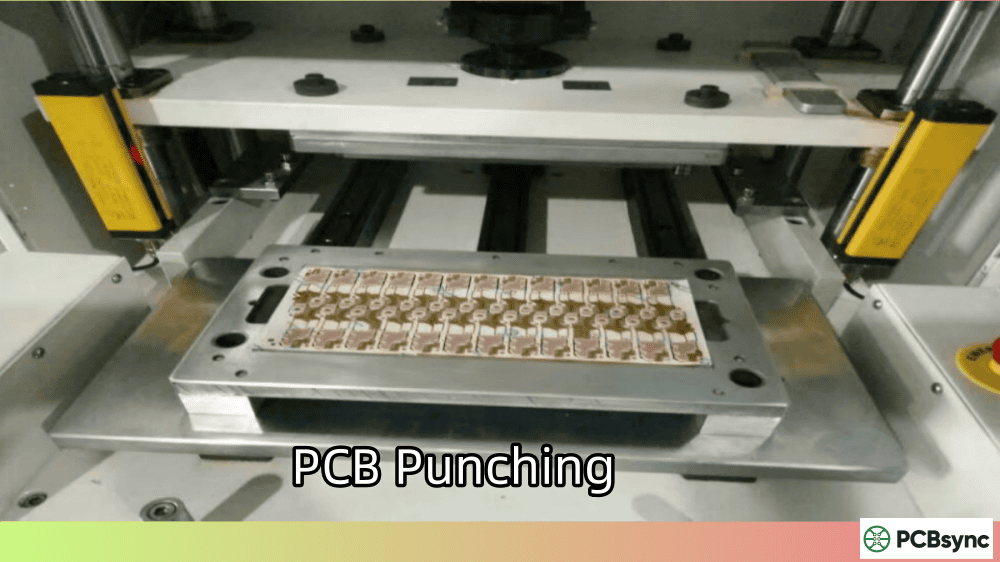
PCB punching (also called die-punch depaneling or die-cutting) is a mechanical separation process where individual printed circuit boards are punched out from a larger production panel using a specially designed die fixture. Think of it like using a cookie cutter—but with extreme precision and hydraulic or pneumatic force.
The punching fixture consists of two main parts: sharp cutting blades on one side and supporting structures on the other. When the panel is placed between these components, the press applies controlled force, and the boards are cleanly separated in a single stroke.
How PCB Punching Works: Step-by-Step Process
Here’s what happens during a typical PCB punching operation:
Panel Loading – The assembled PCB panel is positioned onto the lower die (support structure)
Alignment – Registration pins or vision systems ensure precise positioning
Pressing Action – The upper die descends with controlled force (typically 10-15 tons for standard applications)
Shearing – Sharp blades cut through the remaining web connections or pre-scored areas
Ejection – Singulated boards are released and collected for the next process step
The entire cycle takes just seconds, which is why PCB punching excels in high-volume environments.
When Should You Use PCB Punching?
Not every project suits die-punch depaneling. Based on my experience working with hundreds of different board designs, here’s when PCB punching makes the most sense:
Ideal Applications for PCB Punching
High-volume production runs (typically 10,000+ units)
Understanding how PCB punching stacks up against alternatives helps you make informed decisions. Here’s a detailed comparison based on real-world performance data:
The die (also called the punching mold or fixture) is the heart of any PCB punching operation. Understanding different tooling options helps you optimize for your specific requirements.
Soft Tooling Options
Steel Rule Dies (SRD) are created by bending steel blades into the desired cutting shape and mounting them into a die board. These work great for:
Low to medium-volume production
Quick turnaround (typically 3-5 days)
Budget-conscious projects
Prototype validation before hard tooling investment
Etched Dies are manufactured by chemically etching metal plates to create cutting edges. They’re suitable for:
Lower-volume runs
Applications where extreme precision isn’t critical
Fast prototyping needs
Hard Tooling Options
Precision Steel Dies offer the highest accuracy and longest service life:
Tolerance range: ±0.05mm to ±0.15mm
Lifespan: 200,000+ punching cycles
Ideal for high-volume, long-term production
Higher initial cost, lowest per-unit expense
Carbide Dies provide even greater durability for extremely high volumes or abrasive materials.
Tooling Cost Considerations
Tooling Type
Typical Cost Range
Lifespan
Best Application
Steel Rule Die
$200-$800
20,000-50,000 cycles
Prototypes, low volume
Etched Die
$300-$1,000
30,000-80,000 cycles
Medium volume
Precision Steel
$1,500-$5,000
150,000-300,000 cycles
High volume production
Carbide Die
$3,000-$10,000+
500,000+ cycles
Ultra-high volume
PCB Punching Machine Specifications
Modern PCB punching machines come in various configurations. Here are the key specifications to consider:
Standard Machine Parameters
Parameter
Typical Range
Notes
Pressing Force
5-15 tons
Higher for thicker materials
Working Area
250×300mm to 400×500mm
Match to panel size
Cycle Time
1-3 seconds
Depends on complexity
Positioning Accuracy
±0.05mm
Vision-assisted systems available
Power Source
Pneumatic or hydraulic
Pneumatic more common for lighter work
Noise Level
65-80 dB
Modern machines include dampening
Automation Levels
Manual Systems – Operator loads/unloads panels; suitable for lower volumes
Semi-Automatic Systems – Automated pressing cycle with manual loading; balanced cost/throughput
Fully Automatic Systems – Integrated with conveyor systems; highest throughput, inline SMT compatible
Advantages of PCB Punching
From my hands-on experience, here’s why PCB punching remains popular despite newer technologies:
Speed and Efficiency
Nothing beats punching for raw throughput. A well-tuned system can singulate 6-8 boards per minute, and some high-speed configurations achieve even higher rates. When you’re pushing 50,000 units per month, those seconds add up.
Consistent Quality
Once the die is properly made and the machine is set up, every board comes out identical. There’s no bit wear like with routing, no parameter drift like with lasers. This consistency is golden for quality control.
Clean Operation
Unlike routing (which generates significant FR4 dust), PCB punching produces minimal particulate matter. No vacuum system maintenance, no dust contamination concerns, and a cleaner working environment.
Low Running Costs
After the initial die investment, operational costs are minimal—just electricity, compressed air (for pneumatic systems), and periodic die maintenance.
Environmental Benefits
Low energy consumption (primarily compressed air), dust-free operation, and no cutting fluids make PCB punching environmentally friendly compared to many alternatives.
Limitations and Challenges of PCB Punching
Being honest about limitations helps you avoid costly mistakes:
High Upfront Tooling Investment
Custom dies aren’t cheap, and you’ll need a new one for every different board design. This non-recurring engineering (NRE) cost makes punching impractical for prototypes or frequently changing designs.
Design Change Inflexibility
Once you’ve invested in tooling, design modifications mean new dies. Even small outline changes require tooling updates, unlike software-driven methods like laser or routing.
Mechanical Stress Concerns
The punching action does impart some mechanical stress to boards. For most applications this isn’t problematic, but extremely thin FPCs (under 50μm) or boards with edge-mounted sensitive components require careful consideration.
Die Maintenance Requirements
Blades dull over time, especially when cutting through FR4. Regular sharpening and inspection are essential to maintain cut quality. Neglected dies produce rough edges and can damage boards.
Space Requirements
Punching machines, especially automatic ones, have significant footprints. Smaller facilities may struggle to accommodate the equipment alongside other production lines.
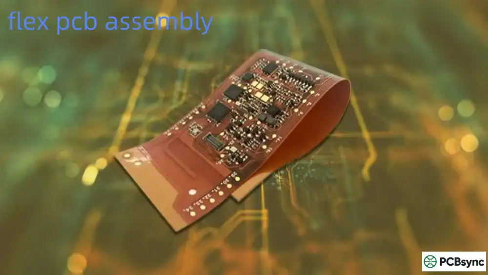
PCB Punching for Flexible Circuits (FPC)
Flexible printed circuits deserve special attention because PCB punching is particularly well-suited for FPC production.
Why FPCs and Punching Work Well Together
Flexible circuits are thin (typically 0.1-0.3mm) and made from polyimide materials that cut cleanly. The punching process is faster than laser cutting for high-volume FPC production and doesn’t create the heat-affected zones that concern some designers.
Common FPC Punching Applications
Coverlay cutting – Punching windows in the protective overlay
Outline profiling – Final board shape separation
Stiffener cutting – FR4 or steel stiffener preparation
EMI shield cutting – Conductive layer singulation
PSA (Pressure Sensitive Adhesive) cutting – Tape and adhesive preparation
FPC Tooling Tolerance Grades
Grade
Tolerance
Typical Application
Standard
±0.15mm
General FPC outlines
Medium Precision
±0.10mm
Connector areas, gold fingers
High Precision
±0.07mm
Fine-pitch connectors
Ultra Precision
±0.05mm
Critical tolerances, ZIF connectors
Design Guidelines for PCB Punching
Designing boards with punching in mind saves headaches during production:
Component Placement Rules
Keep components at least 1.5mm away from punching edges
Orient sensitive components parallel to cut lines when possible
Avoid placing BGA packages directly adjacent to punching zones
Consider stress relief features for critical trace routing near edges
Panel Design Recommendations
Use registration holes for accurate die alignment
Design consistent web widths (typically 2-3mm) between boards
Include breakaway tabs if combining with other separation methods
Add fiducial marks for vision-guided systems
Edge Quality Considerations
Punching produces a slight shear zone at cut edges. For cosmetic applications or boards requiring smooth edges, specify edge requirements in your design documentation.
Quality Control in PCB Punching Operations
Maintaining quality requires systematic approach:
Pre-Production Checks
Verify die sharpness before each production run
Check alignment fixtures for wear
Confirm panel registration accuracy
Validate first-article samples
In-Process Monitoring
Monitor pressing force consistency
Check for edge burrs or irregularities
Verify dimensional accuracy periodically
Watch for signs of die wear
Common Defects and Solutions
Defect
Likely Cause
Solution
Rough edges
Dull blades
Sharpen or replace die
Dimensional drift
Die wear
Recalibrate or refurbish tooling
Board cracking
Excessive force
Reduce pressure, check material
Incomplete separation
Insufficient force
Increase pressure, check die alignment
Edge delamination
Wrong cutting speed
Adjust cycle parameters
Industry Applications of PCB Punching
PCB punching serves diverse industries, each with specific requirements:
Consumer Electronics
High-volume products like smartphones, tablets, and wearables rely on punching for FPC separation. The speed advantage is crucial when producing millions of units.
Automotive Electronics
Dashboard displays, sensor arrays, and control modules often use punched boards. The consistency of punching supports automotive quality standards.
LED Lighting
LED strips and panel lights feature simple, repetitive board shapes perfect for punching. The low per-unit cost aligns with price-sensitive lighting markets.
Medical Devices
Disposable medical electronics (glucose monitors, diagnostic strips) benefit from punching’s clean operation and consistent quality.
Future Trends in PCB Punching Technology
The technology continues evolving:
Smart Die Systems
Newer machines incorporate sensors that monitor die condition in real-time, predicting maintenance needs before quality degrades.
Hybrid Approaches
Combining punching with other methods (punch main separation, route complex areas) optimizes both speed and flexibility.
Improved Automation
Integration with Industry 4.0 systems enables better traceability, predictive maintenance, and production optimization.
Enhanced Precision
Advances in die manufacturing push tolerances tighter, expanding punching’s applicability to more demanding applications.
Useful Resources and Standards
Industry Standards
IPC-2221: Generic Standard on Printed Board Design
IPC-6012: Qualification and Performance Specification for Rigid Printed Boards
IPC-6013: Qualification and Performance Specification for Flexible Printed Boards
When sourcing PCB punching equipment, consider established manufacturers who offer comprehensive support and proven reliability. Request sample processing and reference checks before committing to significant tooling investments.
Frequently Asked Questions About PCB Punching
1. What is the minimum order quantity that makes PCB punching cost-effective?
Generally, PCB punching becomes economically viable starting around 5,000-10,000 units, depending on board complexity and die costs. For simpler dies costing $500-$1,000, even lower volumes can make sense. Calculate your break-even point by dividing tooling cost by the per-unit savings compared to routing or laser cutting. For example, if punching saves $0.10 per board and your die costs $1,000, you break even at 10,000 units.
2. Can PCB punching damage sensitive components on the board?
Yes, punching can stress components near cut edges. The mechanical shock from pressing can crack ceramic capacitors or damage solder joints if components are too close to the punching zone. Best practice is maintaining at least 1.5mm clearance from cut lines to any sensitive components. For particularly fragile assemblies, consider alternative methods like laser depaneling that impart no mechanical stress.
3. How long does a typical punching die last, and what maintenance is required?
A well-made precision steel die typically lasts 150,000-300,000 cycles before requiring significant refurbishment. However, cutting edge sharpness degrades gradually, so periodic sharpening (every 20,000-50,000 cycles depending on material) maintains cut quality. Regular inspection for nicks, chips, or corrosion is essential. Store dies properly in protective cases and keep them clean and lightly oiled to prevent rust.
4. What’s the difference between PCB punching and blanking?
While often used interchangeably, blanking technically refers to a stamping process where the desired part is the piece removed from the sheet, while punching removes unwanted material (the “slug”). In PCB manufacturing, we typically call the process “punching” regardless of which piece is kept. The mechanical principle is identical—both use a die to shear material along a defined profile.
5. Can PCB punching handle boards with irregular or curved outlines?
Yes, but with limitations. Punching dies can be made for curved and irregular shapes, but complex outlines increase die cost and may require larger web areas for proper support during the pressing operation. For extremely intricate shapes with tight internal corners (under 0.5mm radius), routing or laser cutting may be more practical. Simple curves and rounded corners are easily accommodated in punching dies.
Conclusion
PCB punching remains a workhorse technology in electronics manufacturing. While newer methods like laser depaneling grab headlines, the fundamental economics of die-punch separation make it indispensable for high-volume production. The key is matching the method to your specific needs—volume, complexity, tolerance requirements, and budget all factor into the decision.
If you’re producing 10,000+ units of a stable design with moderate tolerance requirements, PCB punching deserves serious consideration. The upfront tooling investment pays dividends through lower per-unit costs, faster cycle times, and consistent quality. Just remember to design with punching in mind, maintain your tooling properly, and partner with experienced suppliers who understand the nuances of the process.
Meta Description Suggestion:
“Learn what PCB punching is and how die-punch depaneling works. Complete guide covering equipment, tooling costs, applications, advantages vs. routing/laser, and design tips for high-volume PCB production.”
Alternative Meta Descriptions:
“PCB punching explained: Discover how die-punch depaneling separates circuit boards efficiently. Compare costs, speeds, and precision with routing and laser methods. Expert guide for manufacturers.”
“What is PCB punching? This complete guide covers die-punch depaneling machines, tooling options, FPC applications, and when to choose punching over routing or laser cutting.”
Inquire: Call 0086-755-23203480, or reach out via the form below/your sales contact to discuss our design, manufacturing, and assembly capabilities.
Quote: Email your PCB files to Sales@pcbsync.com (Preferred for large files) or submit online. We will contact you promptly. Please ensure your email is correct.
Notes: For PCB fabrication, we require PCB design file in Gerber RS-274X format (most preferred), *.PCB/DDB (Protel, inform your program version) format or *.BRD (Eagle) format. For PCB assembly, we require PCB design file in above mentioned format, drilling file and BOM. Click to download BOM template To avoid file missing, please include all files into one folder and compress it into .zip or .rar format.


