Inquire: Call 0086-755-23203480, or reach out via the form below/your sales contact to discuss our design, manufacturing, and assembly capabilities.
Quote: Email your PCB files to Sales@pcbsync.com (Preferred for large files) or submit online. We will contact you promptly. Please ensure your email is correct.
Notes: For PCB fabrication, we require PCB design file in Gerber RS-274X format (most preferred), *.PCB/DDB (Protel, inform your program version) format or *.BRD (Eagle) format. For PCB assembly, we require PCB design file in above mentioned format, drilling file and BOM. Click to download BOM template To avoid file missing, please include all files into one folder and compress it into .zip or .rar format.
After designing hundreds of boards over my career, I can confidently say that PCB marking is one of the most underappreciated aspects of circuit board design. Most engineers obsess over trace widths and via sizes—but then rush through the silkscreen layer in the final hour before sending files to fabrication.
The result? Assembly technicians squinting at illegible text, service engineers playing “guess the component,” and QA teams struggling to trace defective boards back to their origin. Proper PCB marking isn’t glamorous work, but it separates amateur designs from professional-grade boards.
In this comprehensive guide, I’ll walk you through every marking method available, when to use each one, and the design rules that ensure your markings actually serve their purpose.
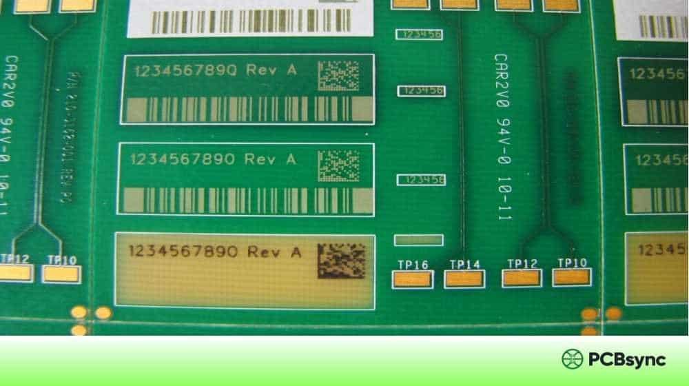
PCB marking refers to all text, symbols, codes, and labels applied to a printed circuit board for identification, traceability, and assembly guidance. These markings can be applied through various methods—from traditional silkscreen printing to laser etching and adhesive labels.
Effective PCB marking serves several critical functions:
Assembly guidance — Reference designators and polarity markers help technicians place components correctly, reducing assembly errors and rework costs.
Traceability — Serial numbers, date codes, and barcodes enable tracking throughout manufacturing, distribution, and field service. When a defect surfaces, you need to trace affected boards back to specific production lots.
Regulatory compliance — Certifications like UL, CE, and RoHS often require specific markings on the board itself. Missing these can delay product launches or block market access entirely.
Field service — Clear component labels and test point markings make troubleshooting and repair significantly faster. Your field technicians will thank you.
Brand identity — Company logos, part numbers, and revision information communicate professionalism and aid inventory management.
Types of PCB Marking: A Complete Overview
Let me break down the main categories of PCB marking you’ll encounter in modern electronics manufacturing.
Silkscreen Markings (Legend Layer)
The silkscreen—also called the legend layer—is the most common form of PCB marking. It’s a layer of non-conductive epoxy ink applied to the board surface, typically in white (on green solder mask) or black (on white/light-colored boards).
Data Matrix is the industry standard for PCB traceability because it offers the highest data density in the smallest footprint. The Electronic Components Industry Association (ECIA) specifically recommends Data Matrix for labeling small electronic components.
QR codes are better suited for consumer-facing applications where end-users might scan the code with smartphones—think product registration or user manual links.
Laser Marking
Laser marking has emerged as the preferred method for permanent, high-contrast PCB identification. Unlike ink-based methods, laser marks are:
Permanent and tamper-resistant
Resistant to chemicals, solvents, and cleaning processes
Extremely precise (down to 0.1mm line widths)
Environmentally friendly (no inks or solvents)
Laser marking works by either ablating the solder mask to expose the underlying substrate or by altering the surface texture to create contrast. Different laser types serve different purposes:
Laser Type
Wavelength
Best For
Typical Applications
CO2
10,600 nm
Organic materials
Solder mask marking, FR4 etching
Fiber (Nd:YAG)
1,064 nm
Metals, ceramics
Exposed copper, metal substrates
UV
355 nm
Heat-sensitive materials
Fine markings, clean-room environments
MOPA Fiber
Variable
Versatile marking
Color marking on metals, high-speed production
The cost of laser marking has dropped significantly—bulk marking now runs approximately $0.02 per board compared to $0.07-0.09 for ink-based labels.
Adhesive Labels
For applications requiring variable data or when direct marking isn’t feasible, adhesive labels remain a viable option.
Polyimide labels are the industry standard for PCB applications. They withstand:
Temperatures up to 300°C (surviving reflow soldering)
Chemical exposure from cleaning agents
Mechanical abrasion during handling
Standard polyimide labels offer print resolutions up to 600 DPI with minimum sizes of 4mm × 4mm. They’re particularly useful for:
Post-assembly serialization
Customer-specific marking requirements
Retrofit traceability on existing inventory
Copper Layer Marking
Sometimes markings are etched directly into the copper layer. This approach is typically reserved for:
Part numbers on inner layers (for identification during fabrication)
UL recognition marks required in copper
Permanent identification that can’t be covered by components
The downside? Copper marking consumes valuable routing real estate and can only be done during initial fabrication.
Understanding the manufacturing process helps you design better markings. Here’s how the main methods work in practice.
Silkscreen Printing Methods
Manual Screen Printing — The traditional method uses a mesh screen with a stencil. Ink is pushed through the open areas onto the PCB surface. It’s cost-effective for simple designs but limited in resolution (minimum line widths around 7-8 mils).
Liquid Photo Imaging (LPI) — A photosensitive epoxy is applied to the board, then exposed to UV light through a film with the desired pattern. Unexposed areas wash away, leaving precise markings. LPI achieves finer resolution (down to 4 mils) but costs more and takes longer.
Direct Legend Printing (DLP) — Inkjet technology prints directly onto the PCB surface without stencils or films. It’s fast, flexible, and eliminates tooling costs. Resolution typically falls between screen printing and LPI. DLP is ideal for prototypes and variable data but may not match LPI’s durability for harsh environments.
Method
Min. Line Width
Setup Cost
Per-Board Cost
Best For
Screen Printing
7 mils (0.18mm)
Low
Low
High-volume, simple designs
LPI
4 mils (0.10mm)
Medium
Medium
High-density, detailed markings
DLP/Inkjet
3-5 mils
Very Low
Low-Medium
Prototypes, variable data
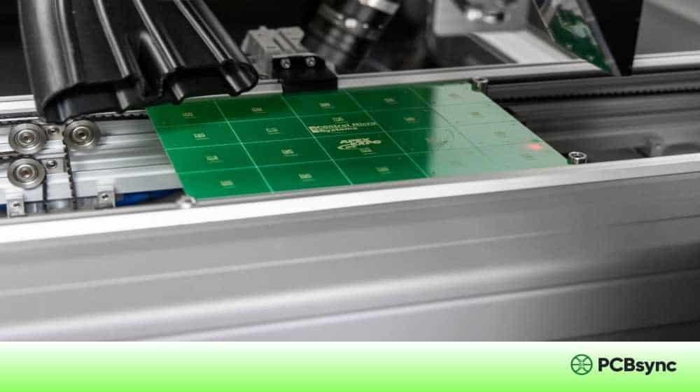
Laser Marking Process
Modern laser marking systems integrate directly into SMT lines. The typical workflow:
Board enters the laser marking station via conveyor
Vision system locates fiducial markers for precise positioning
Marking data (serial numbers, barcodes, logos) is uploaded from the production database
Laser executes the marking pattern in milliseconds
Optional verification camera confirms mark quality
Board exits to the next station
Cycle times are impressively fast—a typical serial number plus Data Matrix code takes 0.5-1.5 seconds per board.
PCB Silkscreen Design Guidelines
Getting your silkscreen right requires attention to specific design rules. Here’s what I’ve learned works best.
Font Size and Line Width Requirements
Parameter
Minimum
Recommended
Notes
Font height
0.8mm (32 mils)
1.0-1.5mm (40-60 mils)
Smaller risks illegibility
Line/stroke width
0.15mm (6 mils)
0.15-0.2mm (6-8 mils)
Too thin won’t print; too thick blurs text
Character spacing
0.1mm (4 mils)
0.15mm (6 mils)
Prevents characters from merging
Pro tip: Use simple sans-serif fonts like Arial or Helvetica. Serif fonts and decorative typefaces look terrible at small sizes and often fail to print cleanly.
Clearance Rules
Maintaining proper clearances prevents PCB manufacturing issues and ensures markings remain visible after assembly.
From
To
Minimum Clearance
Silkscreen
Solder pads
0.15mm (6 mils)
Silkscreen
Vias
0.15mm (6 mils)
Silkscreen
Board edge
0.5mm (20 mils)
Silkscreen
Component body
0.2mm (8 mils)
Critical rule: Never place silkscreen over exposed pads. Ink on pads compromises solderability and can cause assembly defects.
Orientation and Placement Best Practices
After watching assembly technicians struggle with poorly-designed silkscreens, I’ve adopted these practices:
Consistent orientation — Keep all text readable from one or two directions maximum (typically 0° and 90°). Having technicians constantly rotate the board wastes time and increases error risk.
Proximity to components — Place reference designators within 0.75mm of their associated component, but outside the component footprint. The designator should remain visible after the component is placed.
Hierarchy of importance — When space is limited, prioritize markings in this order:
Reference designators (essential for assembly)
Polarity markers (prevents orientation errors)
Pin 1 indicators
Test points
Board identification
Logos and decorative elements
Avoid small discrete parts — For 0402 and smaller packages, skip the component outline entirely. The silkscreen bump can actually interfere with reflow soldering and contribute to tombstoning.
Reference Designators: The Standard System
Reference designators follow industry conventions defined by ASME Y14.44-2008 and IEEE 315. Using standard designators ensures your documentation is universally understood.
Letter
Component Type
Example
R
Resistor
R1, R47
C
Capacitor
C1, C105
L
Inductor
L1, L3
D
Diode
D1, D12
Q
Transistor
Q1, Q8
U
Integrated circuit
U1, U24
J
Connector (jack)
J1, J5
P
Plug/connector
P1, P3
SW
Switch
SW1, SW4
F
Fuse
F1, F2
Y
Crystal/oscillator
Y1, Y2
T
Transformer
T1, T2
TP
Test point
TP1, TP15
FID
Fiducial marker
FID1, FID3
Number designators sequentially within each type, typically from left-to-right, top-to-bottom across the board. Your CAD software can automate this annotation process.
Common PCB Marking Mistakes to Avoid
I’ve reviewed enough designs to compile a greatest-hits list of silkscreen failures:
Text over pads — The most common error. Always run a DRC check specifically for silkscreen-to-pad conflicts.
Illegible font sizes — Going below 0.8mm height might fit more text, but nobody can read it. If you can’t fit the text, abbreviate or relocate—don’t shrink.
Missing polarity markers — Electrolytic capacitors, diodes, and LEDs absolutely require clear polarity indication. A missing marker can turn a $5 component into a warranty claim.
Inconsistent orientation — Text at random angles forces technicians to rotate the board constantly. Pick one or two orientations and stick to them.
Silkscreen under components — Any text placed under a component body becomes invisible after assembly. If you need labels visible post-assembly, place them adjacent to components.
Ignoring manufacturer capabilities — Some fabricators can’t hit 4-mil line widths reliably. Check your vendor’s specs before finalizing the design.
Forgetting the bottom side — Double-sided assemblies need silkscreen on both sides. Remember to mirror bottom-layer text in your Gerber output.
IPC Standards for PCB Marking
Several IPC standards govern PCB marking requirements:
Data Matrix generators: Most EDA software includes built-in generators
Reference designator lists: Your EDA tool’s component library
Manufacturer Resources:
Contact your PCB fabricator for their specific silkscreen capabilities
Assembly houses often publish DFM guidelines including marking requirements
Frequently Asked Questions About PCB Marking
1. What’s the difference between silkscreen and solder mask?
Solder mask is the colored coating (typically green) that protects copper traces and prevents solder bridges. Silkscreen is the text and symbols printed on top of the solder mask for identification purposes. They’re separate layers applied at different manufacturing stages.
2. Can laser marking damage the PCB or affect circuit performance?
When properly applied, laser marking doesn’t penetrate beyond the solder mask layer and has no effect on circuit performance. The laser parameters (power, speed, frequency) are tuned to mark only the surface material. However, avoid laser marking directly on high-speed signal traces—the altered surface could theoretically affect impedance, though this is rarely an issue in practice.
3. Which barcode format should I use for PCB traceability?
For most PCB applications, Data Matrix (ECC 200) is the recommended choice. It offers the best data density for small spaces and has robust error correction. Use Code 128 for simple serial numbers when scanner compatibility with older equipment matters. Reserve QR codes for consumer-facing applications where smartphone scanning is expected.
4. What’s the minimum silkscreen font size that will actually print clearly?
The practical minimum is 0.8mm (32 mils) font height with 0.15mm (6 mils) stroke width. You can technically go smaller with DLP printing (down to 0.5mm), but readability suffers significantly. I recommend 1.0mm (40 mils) as a default target—it’s readable without magnification and prints reliably across most fabricators.
5. Do I need silkscreen on both sides of a double-sided PCB?
If both sides have components, yes. Each component needs its reference designator visible for assembly. Even if one side has only a few components, add silkscreen—the cost difference is negligible, and the assembly team will appreciate it. Just remember to mirror the bottom-layer silkscreen in your Gerber output.
Final Thoughts on PCB Marking
Good PCB marking is invisible when done right—it just works. Assembly runs smoothly, service calls resolve faster, and nobody complains about illegible text or missing polarity markers.
The key takeaways:
Choose the right marking method for your application (silkscreen for most, laser for traceability, labels for variable data)
Follow established size and clearance rules—they exist for good reasons
Use standard reference designators consistently
Never sacrifice legibility for aesthetics
Verify your silkscreen layer before releasing to fabrication
Take an extra thirty minutes on your silkscreen layer. Your manufacturing partners, field service team, and future self will thank you.
Inquire: Call 0086-755-23203480, or reach out via the form below/your sales contact to discuss our design, manufacturing, and assembly capabilities.
Quote: Email your PCB files to Sales@pcbsync.com (Preferred for large files) or submit online. We will contact you promptly. Please ensure your email is correct.
Notes: For PCB fabrication, we require PCB design file in Gerber RS-274X format (most preferred), *.PCB/DDB (Protel, inform your program version) format or *.BRD (Eagle) format. For PCB assembly, we require PCB design file in above mentioned format, drilling file and BOM. Click to download BOM template To avoid file missing, please include all files into one folder and compress it into .zip or .rar format.


