Inquire: Call 0086-755-23203480, or reach out via the form below/your sales contact to discuss our design, manufacturing, and assembly capabilities.
Quote: Email your PCB files to Sales@pcbsync.com (Preferred for large files) or submit online. We will contact you promptly. Please ensure your email is correct.
Notes: For PCB fabrication, we require PCB design file in Gerber RS-274X format (most preferred), *.PCB/DDB (Protel, inform your program version) format or *.BRD (Eagle) format. For PCB assembly, we require PCB design file in above mentioned format, drilling file and BOM. Click to download BOM template To avoid file missing, please include all files into one folder and compress it into .zip or .rar format.
If you’ve ever wondered what makes a printed circuit board reliable enough to work flawlessly in your smartphone, medical device, or aerospace system, the answer often comes down to PCB plating. I’ve spent years working with circuit boards, and I can tell you that plating is one of those processes that separates a board that works from one that fails in the field.
This guide breaks down everything you need to know about PCB plating—from the fundamental processes to advanced techniques like pattern plating and edge plating. Whether you’re a design engineer specifying your first multilayer board or a procurement specialist trying to understand what you’re buying, you’ll find practical information here.
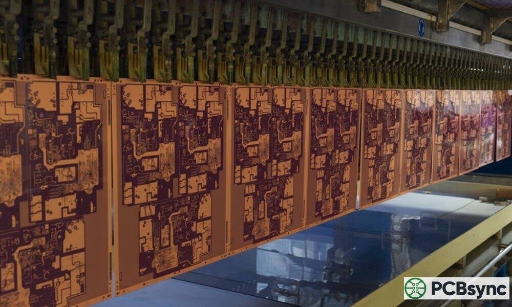
PCB plating is the process of depositing a thin metal layer onto the surfaces and holes of a printed circuit board. The primary metals used include copper, gold, silver, nickel, and tin. Each serves a specific purpose in protecting the board and enabling reliable electrical connections.
Here’s the thing most people miss: without proper plating, copper traces oxidize within weeks. Oxidized copper doesn’t solder well, and poor solder joints are the number one cause of field failures in electronics. Plating isn’t optional—it’s what makes your board manufacturable and reliable.
The Core Functions of PCB Plating
Function
What It Does
Why It Matters
Corrosion Protection
Prevents copper oxidation
Extends shelf life and operational lifespan
Electrical Conductivity
Creates paths between layers
Enables multilayer board functionality
Solderability
Provides wettable surface for solder
Ensures strong component connections
Wear Resistance
Protects contact surfaces
Critical for edge connectors and gold fingers
Signal Integrity
Maintains impedance consistency
Essential for high-speed designs
From a practical standpoint, proper PCB plating directly impacts three things you care about: yield during assembly, reliability in the field, and overall product cost. Get plating wrong, and you’re looking at rework, returns, and warranty claims.
Understanding the PCB Plating Process Step-by-Step
The plating process follows a logical sequence that builds up copper from the initial seed layer to the final thickness specification. Here’s what actually happens in a typical fabrication shop.
Step 1: Drilling and Desmearing
After drilling through-holes and vias, resin smear from the drilling process coats the hole walls. This smear must be removed completely, or the copper won’t adhere properly. Most shops use either permanganate chemical treatment or plasma desmearing.
Step 2: Surface Preparation and Cleaning
The board goes through alkaline cleaning to remove oils, followed by micro-etching to create surface roughness. This roughness is critical—copper needs something to grip onto. Skip this step, and you’ll see delamination down the road.
Step 3: Catalyzation (Activation)
For electroless plating to work, the non-conductive hole walls need activation. A palladium-tin catalyst solution is applied, which deposits catalyst particles that will initiate copper deposition. This is where the magic of plating non-conductive surfaces happens.
Step 4: Electroless Copper Deposition
This autocatalytic process deposits a thin copper seed layer (typically 0.5-1.0 μm) without external electrical current. The chemical reaction deposits copper ions onto any surface containing the catalyst.
The electroless layer serves as the foundation for everything that follows. It’s thin, but it creates the conductive path needed for electrolytic plating.
Step 5: Electrolytic Copper Plating
With a conductive seed layer in place, the board acts as a cathode in an acid copper sulfate bath. DC current drives copper ions from the anode to deposit onto the board surfaces and hole walls. This builds up copper to the required thickness—typically 18-25 μm for standard boards, or 25+ μm for high-reliability applications.
Key process parameters:
Parameter
Typical Range
Impact if Out of Spec
Current density
1.5-3.0 A/dm²
Too high: burning, rough deposits; Too low: slow plating, poor coverage
Bath temperature
20-25°C
Higher temp: faster plating but rougher; Lower: slower, may affect throwing power
Copper concentration
60-80 g/L
Low: reduced plating rate; High: possible nodule formation
Sulfuric acid
180-220 g/L
Affects conductivity and throwing power
Chloride
40-80 ppm
Critical for additive function; too low causes dull deposits
Throwing power is a critical concept here. It describes how well the plating solution deposits copper into holes versus on surfaces. Higher throwing power means more uniform plating in high-aspect-ratio holes. Additives (brighteners, levelers, carriers) are used to optimize throwing power for specific hole geometries.
Pulse plating vs. DC plating: For challenging geometries like high-aspect-ratio holes or blind vias, pulse plating offers advantages. By alternating current on/off or forward/reverse, pulse plating allows ion concentration to recover near the plating surface, resulting in more uniform deposits. Some advanced processes use pulse-periodic-reverse (PPR) plating for via filling applications.
Step 6: Final Processing
Depending on the manufacturing method (pattern or panel plating), additional steps include photoresist application, imaging, tin plating as an etch resist, and final etching to define the circuit pattern.
Different applications require different plating approaches. Here’s what each method offers and when to use it.
Through-Hole Plating (PTH)
Through-hole plating connects the copper layers of a multilayer board through drilled holes. The process deposits copper onto the non-conductive hole walls, creating electrical pathways between layers.
Wrap plating extension: minimum 0.025 mm onto land surface
No voids allowed in Class 3 boards
Selective Plating (Finger Plating)
Gold fingers, edge connectors, and contact areas require selective plating with precious metals. These areas get thicker gold (typically 0.5-1.5 μm hard gold over 2.5-5.0 μm nickel) while the rest of the board receives standard finish.
This method is more expensive but essential for boards with edge connectors that need to withstand thousands of insertion cycles.
Brush Plating
For repairs, rework, or prototype modifications, brush plating applies metal locally using a handheld anode wrapped in absorbent material soaked in plating solution. It’s not for production, but it saves scrapping expensive boards during development.
Electroless Plating
Beyond the seed layer application, electroless processes are used for final surface finishes like ENIG (Electroless Nickel Immersion Gold). These chemical deposition methods don’t require electrical current, making them suitable for coating complex geometries uniformly.
Pattern Plating vs. Panel Plating: A Critical Manufacturing Decision
This is where manufacturing engineers earn their paychecks. The choice between pattern plating and panel plating affects trace definition, copper distribution, impedance control, and overall board cost.
What Is Pattern Plating?
Pattern plating deposits copper only on the circuit pattern areas after photoresist imaging. The sequence goes:
Panel plating deposits copper uniformly across the entire panel surface before any imaging. The sequence differs:
Apply electroless copper seed layer
Electroplate copper over entire panel
Laminate and image dry film photoresist (positive image)
Etch away unwanted copper
Strip photoresist
Head-to-Head Comparison
Factor
Pattern Plating
Panel Plating
Trace Definition
Better (only base copper etched)
Poorer (plated + base copper etched)
Fine-Line Capability
3% width variation
10-15% width variation
Copper Distribution
Varies with pattern density
Uniform across panel
Impedance Control
Better for controlled impedance
More variation expected
Process Cost
Higher (more steps)
Lower (simpler process)
Best Applications
Fine-pitch, HDI, RF boards
Standard boards, high-current designs
When to Use Each Method
Choose pattern plating for:
Fine-pitch components (< 0.5 mm pitch)
Controlled impedance traces
High-density interconnect (HDI) boards
RF and high-frequency applications
Choose panel plating for:
Standard pitch designs
Power boards requiring thicker copper
Cost-sensitive applications
Designs without tight impedance requirements
The width variation difference is significant. With pattern plating, a 6-mil trace stays very close to 6 mils. With panel plating, that same trace might vary from 5.4 to 6.8 mils because you’re etching through more copper. For impedance-controlled lines where every mil matters, pattern plating is usually the right call.
PCB Plating Materials: Choosing the Right Metal
The metal you plate with depends on what you need that surface to do. Here’s a practical breakdown.
Copper
Copper is the workhorse of PCB plating. Its electrical conductivity (5.96×10⁷ S/m) is second only to silver, and it’s far more cost-effective.
Copper Specification
Typical Value
Electrical conductivity
5.96×10⁷ S/m
Standard foil weights
0.5 oz, 1 oz, 2 oz per sq ft
PTH minimum thickness
18-25 μm
Heavy copper threshold
> 3 oz per sq ft
Gold
Gold plating serves two main purposes: preventing oxidation and providing durable contact surfaces.
Immersion gold (ENIG): 0.05-0.1 μm over 3-6 μm nickel
Hard gold (electrolytic): 0.5-1.5 μm over nickel for edge connectors
Soft gold: For wire bonding applications
Gold doesn’t tarnish, making it ideal for boards that will sit in inventory before assembly.
Nickel
Nickel acts as a barrier layer between copper and gold, preventing copper migration that would contaminate the gold surface. It also adds hardness to gold finger surfaces.
Silver
Immersion silver provides excellent solderability and maintains signal integrity at high frequencies better than ENIG. The downside: it tarnishes if exposed to sulfur compounds, limiting shelf life to about 6 months.
Tin
Lead-free tin plating offers good solderability at lower cost than gold or silver. However, tin whisker growth remains a concern for high-reliability applications. Tin whiskers are microscopic metal filaments that can grow spontaneously from tin-plated surfaces, potentially causing short circuits in dense electronic assemblies.
Mitigation strategies for tin whiskers:
Use matte tin instead of bright tin (larger grain structure)
Apply nickel underplate as a diffusion barrier
Consider tin-lead alloys where RoHS doesn’t apply
Maintain minimum tin thickness of 2 μm
Material Selection Decision Matrix
Choosing the right plating material requires balancing multiple factors. Use this matrix as a starting point:
The reality is that most designs don’t need exotic finishes. ENIG handles 80% of applications well. Reserve specialized finishes for designs that genuinely require them.
Side Plating vs. Castellated Edges: Edge Connection Techniques
When boards need to connect through their edges—whether for EMI shielding or module mounting—two techniques dominate: side plating and castellated holes.
Side Plating (Edge Plating)
Side plating deposits continuous copper along the PCB perimeter from top to bottom surface. The copper wraps around the board edge, creating a conductive path.
Applications:
EMI/EMC shielding (grounding the edge to an enclosure)
Non-connection layers: maintain 800 μm clearance from edge
Gaps needed for panel tabs during manufacturing
Castellated Holes (Plated Half-Holes)
Castellated holes are plated through-holes cut in half at the board edge, creating half-moon shaped plated surfaces. They’re designed for surface-mount soldering of one board onto another.
Applications:
WiFi/Bluetooth module mounting
Daughter boards and breakout modules
Board-to-board connections without connectors
Creating PCB “components” that solder like SMD parts
Design requirements:
Minimum hole diameter: 0.6 mm (some fabs accept 0.4 mm)
Burrs: Metal fragments from routing can obstruct holes. Quality fabs use modified processes to minimize this.
Misalignment: If the router doesn’t hit hole centers precisely, castellations end up asymmetric. This reduces solder fillet area.
Copper pull-away: The routing tool can catch and tear copper from the unsupported hole wall.
Pro tip: When designing modules with castellations, specify that your fabricator use a two-stage routing process. The first pass creates the rough edge; the second pass cleans up the castellations with a fresh bit.
Comparison Table
Characteristic
Side Plating
Castellated Holes
Coverage
Continuous edge metallization
Discrete half-holes
Primary use
Shielding, grounding
Module mounting
Connection type
Compression/contact
Solder joint
Design complexity
Lower
Higher (requires hole alignment)
Common defects
Copper peeling
Burrs, misalignment
Surface finish
ENIG recommended
ENIG required for round castellations
Common PCB Plating Defects and How to Prevent Them
In my experience, most plating defects trace back to process control issues. Here’s what to watch for and how to fix it.
Voids in Plated Through-Holes
What it looks like: Missing copper in the hole barrel, visible as gaps or holes in cross-section.
Causes:
Air bubbles during electroless plating
Contamination in plating bath
Inadequate activation (catalyst coverage)
High aspect ratio holes (> 6:1)
Prevention:
Improve agitation during plating
Maintain bath chemistry within spec
Consider direct metallization for high-reliability boards
Keep aspect ratios below 6:1 when possible
IPC acceptance criteria:
Class 2: Max 5% of holes with voids, each void < 5% of hole length
Class 3: No voids allowed
Uneven Plating Thickness
What it looks like: Copper thicker in some areas than others, often thicker at board edges and thinner in center.
Causes:
Non-uniform current distribution
Poor copper balance in design
Improper anode configuration
Bath chemistry out of specification
Prevention:
Use auxiliary anodes for complex designs
Design with copper balance in mind (thieving)
Maintain current density within optimal range (1.5-3.0 A/dm²)
Regular bath maintenance and analysis
Poor Adhesion (Peeling)
What it looks like: Copper lifting from substrate, especially at edges or near holes.
Causes:
Inadequate surface preparation
Contamination before plating
Insufficient electroless copper thickness
Residual desmear chemicals
Prevention:
Proper cleaning and micro-etching
Verify rinse water quality
Monitor electroless bath activity
Complete desmear neutralization
Nodules and Pitting
What it looks like: Bumps (nodules) or depressions (pits) in plated surface.
Wrap plating is the copper that extends from the hole barrel onto the land area. It’s critical for reliability because it creates a mechanical and electrical connection between the plated hole and the surface copper.
What it looks like: Separation between barrel copper and land copper, visible as a dark line or actual gap in cross-section.
Causes:
Insufficient wrap (less than 25 μm extension)
Poor adhesion between electroless and electrolytic copper
IPC-6012B requirement: Wrap plating must extend minimum 0.025 mm (1 mil) from hole wall onto surrounding land area for Class 3 boards.
Pattern Plating-Specific Defects
Pattern plating introduces additional failure modes related to the photoresist process:
Mushrooming: Copper plates under the photoresist edges, creating overhanging “mushroom” shapes. This happens when resist adhesion is poor or plating time is excessive.
Skip plating: Areas that should be plated remain bare. Usually caused by resist residue, contamination, or inadequate activation.
Line width variation: Caused by resist undercut during development or excessive plating time that thickens lines beyond specification.
Troubleshooting Workflow
When plating defects occur, follow this systematic approach:
Document the defect: Photos, location on board, which boards affected
Check process parameters: Compare actual vs. specified values for temperature, current density, time
Analyze bath chemistry: Get a Hull cell test and full chemical analysis
Review recent changes: New bath makeup, maintenance, different operators
Examine cross-sections: Quantify the defect severity
Implement corrective action: Address root cause, not just symptoms
Verify correction: Run test panels before production
IPC Standards for PCB Plating: What You Need to Know
IPC standards define the quality requirements that separate reliable boards from problematic ones. Here are the key standards relevant to plating.
IPC-6012: Qualification and Performance Specification for Rigid PCBs
This standard specifies copper thickness requirements, plating quality criteria, and testing methods.
Requirement
Class 2
Class 3
Minimum PTH copper
18 μm
25 μm
Plating voids
Limited allowed
Not allowed
Wrap plating
Required
Required with positive etchback
Surface copper tolerance
Per spec
Tighter tolerance
IPC-A-600: Acceptability of Printed Boards
The visual inspection standard that defines what’s acceptable and what’s not for plating quality, including:
Void size and distribution
Copper thickness verification
Plating adhesion
Surface defects
IPC-TM-650: Test Methods Manual
Contains the actual test procedures for verifying plating quality:
2.4.18.1: Tensile strength and elongation
2.6.8: Solder shock (thermal stress)
Microsection analysis methods
Practical Tips for Better PCB Plating Results
After reviewing dozens of board designs and troubleshooting plating issues, here are my top recommendations:
Design Stage
Balance your copper—Add copper thieving to achieve uniform plating distribution. Thieving patterns (dummy copper features) in low-density areas help equalize current distribution across the panel.
Keep aspect ratios reasonable—Below 6:1 for standard processes, below 10:1 for advanced. Calculate aspect ratio as board thickness divided by minimum hole diameter.
Specify the right class—Don’t over-specify (costs more) or under-specify (reliability risk). Class 2 handles most commercial applications; Class 3 is for life-critical systems.
Consider thermal requirements—High-current areas may need heavier copper. Use IPC-2152 charts to determine required trace widths and copper weights.
Design for testability—Include test coupons for plating verification if your fabricator doesn’t add them automatically.
Copper Balance and Thieving Strategies
Unbalanced copper distribution is one of the most common causes of plating variation. Here’s how to address it:
Problem indicators:
Large ground planes adjacent to fine-pitch areas
One side of board has high copper density, other side has sparse traces
Isolated pads far from other features
Solutions:
Add thieving copper (cross-hatched patterns) in sparse areas
Use hatched fills instead of solid pours where appropriate
Request your fabricator add automated thieving
Consider panel plating for severely unbalanced designs
Quantifying copper balance: Some CAD tools calculate plating index—a measure of copper distribution uniformity. Ask your fabricator what plating index they can handle without adding copper balancing.
Communication with Your Fabricator
Specify critical dimensions—Call out minimum copper thickness requirements explicitly in your fabrication notes.
Identify controlled impedance traces—These may need pattern plating. Provide target impedance, tolerance, and reference stackup.
Discuss edge plating early—It affects panelization and routing. Edge plating requires routing before plating, which limits panel layout options.
Request cross-section reports—Verify plating thickness on first articles. Good fabricators provide this automatically for Class 3 boards.
Share your application environment—Thermal cycling requirements, humidity exposure, and expected lifetime help the fabricator recommend appropriate processes.
Quality Verification
Review microsections—They show actual plating thickness and quality. Look for uniform copper, no voids, adequate wrap plating.
Check for voids—X-ray inspection for production, destructive cross-section for qualification. Focus on highest aspect ratio holes.
Verify surface finish thickness—Especially for ENIG gold thickness (0.05-0.1 μm) and nickel thickness (3-6 μm). Both too thin and too thick cause problems.
Test adhesion—Tape test per IPC-TM-650 for surface finish adhesion. Solder float test for overall plating integrity.
Perform electrical testing—Continuity and isolation testing catches plating opens and shorts that visual inspection misses.
Useful Resources for PCB Plating
Here are some resources I’ve found helpful over the years:
Standards and Specifications
IPC-6012: IPC Store — Performance spec for rigid PCBs. Essential reading for understanding plating requirements by class.
IPC-A-600: IPC Store — Acceptability of printed boards. The definitive guide for visual inspection criteria.
What is the minimum copper thickness required for plated through-holes?
Per IPC-6012, the minimum copper thickness for plated through-holes is 18 μm for Class 2 boards and 25 μm for Class 3 boards. Most fabricators target 20-25 μm as their internal standard to provide margin above the minimum. For high-reliability applications or boards that will see multiple reflow cycles, specifying 25 μm minimum is recommended regardless of class.
What’s the difference between electroless and electrolytic copper plating?
Electroless plating uses chemical reduction to deposit copper without external electrical current. It’s used to create the initial thin conductive layer (0.5-1.0 μm) on non-conductive hole walls. Electrolytic plating uses DC current to drive copper ions from solution onto the board, building up thickness rapidly to the final specification. Both processes are required for through-hole plating—electroless creates the seed layer, electrolytic builds the thickness.
When should I use pattern plating instead of panel plating?
Use pattern plating when you need fine-line traces (< 6 mil trace/space), controlled impedance, or minimal copper thickness variation. It’s the standard choice for high-density interconnect (HDI) and high-frequency designs. Use panel plating for standard designs where trace width tolerance isn’t critical, or for heavy copper boards where you want maximum copper uniformity across the panel.
How do I prevent plating voids in high aspect ratio holes?
For holes with aspect ratios above 6:1, consider these approaches: (1) Use direct metallization instead of electroless copper for better hole wall coverage, (2) Implement pulse plating which improves throwing power into deep holes, (3) Increase agitation in plating baths, (4) Consider back-drilling oversized holes and re-drilling to final size, (5) Work with your fabricator to optimize their process for your specific aspect ratio requirements.
What surface finish is best for boards that will sit in inventory?
ENIG (Electroless Nickel Immersion Gold) provides the longest shelf life—typically 12 months or more without degradation. The gold layer prevents oxidation of the underlying nickel. Immersion silver is a good alternative for high-frequency applications but has shorter shelf life (6 months) due to tarnishing. OSP (Organic Solderability Preservative) is lowest cost but has limited shelf life (3-6 months) and may not withstand multiple reflow cycles.
Conclusion
PCB plating is the foundation of reliable circuit board manufacturing. From the initial electroless seed layer through final surface finish, each step builds on the previous to create boards that conduct electricity efficiently, solder reliably, and survive years of operation.
The key takeaways:
Process matters: Electroless copper creates the foundation; electrolytic copper builds the structure
Method selection impacts quality: Pattern plating for fine features, panel plating for standard designs
Material choice depends on application: Copper for conductivity, gold for contacts, nickel as a barrier
Standards exist for good reasons: IPC specifications represent decades of industry experience
Defects are preventable: Most plating problems trace back to process control issues
Whether you’re designing your first board or your hundredth, understanding plating helps you make better decisions about specifications, communicate more effectively with fabricators, and troubleshoot issues when they arise.
Inquire: Call 0086-755-23203480, or reach out via the form below/your sales contact to discuss our design, manufacturing, and assembly capabilities.
Quote: Email your PCB files to Sales@pcbsync.com (Preferred for large files) or submit online. We will contact you promptly. Please ensure your email is correct.
Notes: For PCB fabrication, we require PCB design file in Gerber RS-274X format (most preferred), *.PCB/DDB (Protel, inform your program version) format or *.BRD (Eagle) format. For PCB assembly, we require PCB design file in above mentioned format, drilling file and BOM. Click to download BOM template To avoid file missing, please include all files into one folder and compress it into .zip or .rar format.


