Inquire: Call 0086-755-23203480, or reach out via the form below/your sales contact to discuss our design, manufacturing, and assembly capabilities.
Quote: Email your PCB files to Sales@pcbsync.com (Preferred for large files) or submit online. We will contact you promptly. Please ensure your email is correct.
Notes: For PCB fabrication, we require PCB design file in Gerber RS-274X format (most preferred), *.PCB/DDB (Protel, inform your program version) format or *.BRD (Eagle) format. For PCB assembly, we require PCB design file in above mentioned format, drilling file and BOM. Click to download BOM template To avoid file missing, please include all files into one folder and compress it into .zip or .rar format.
If you’ve ever worked on a PCB production line, you know that moment when everything is assembled, tested, and ready—but the boards are still connected in a panel. That’s where PCB depaneling comes in. It’s the final step that separates your carefully manufactured circuit boards into individual units ready for integration.
I’ve seen engineers spend weeks optimizing their SMT process only to damage boards during separation. The wrong depaneling method can crack solder joints, stress components, or leave ugly edges that won’t fit the enclosure. After fifteen years of working with electronics manufacturing, I can tell you that depaneling is often the most underestimated step in the entire production process.
The evolution of electronic devices toward smaller form factors and higher component density has made proper depaneling more critical than ever. When components are placed within a millimeter of board edges and solder joints are microscopic, the stress from separation can make or break product reliability. A 2023 industry survey found that approximately 12% of PCB assembly defects could be traced back to the depaneling process—a significant number that directly impacts yield and profitability.
This guide breaks down the seven main PCB depaneling methods so you can pick the right one for your project. Whether you’re manufacturing LED lighting panels, medical monitoring devices, or consumer electronics, understanding these methods will help you optimize quality, reduce costs, and minimize production headaches.
PCB depaneling (also called depanelization or singulation) is the process of separating individual printed circuit boards from a larger manufacturing panel. During production, multiple PCBs are grouped together on a single panel to increase throughput and reduce handling during the SMT assembly process. Once assembly and testing are complete, these boards need to be separated.
The challenge? Every depaneling method creates some level of mechanical stress. The goal is to minimize that stress while maintaining production speed and cost efficiency.
Why Panelization Matters for Depaneling
Before we dive into depaneling methods, it’s worth understanding why your panelization design directly impacts your depaneling options:
Panel size and board count affect handling and cycle times
Board geometry determines which methods are even possible
Component placement near edges limits your options
Material type (FR-4, aluminum, flex) requires different approaches
The depaneling method should be considered during PCB design—not as an afterthought.
The 7 PCB Depaneling Methods Compared
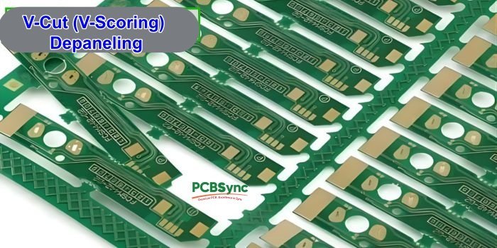
1. V-Cut (V-Scoring) Depaneling
V-Cut is the workhorse of PCB depaneling. During panel fabrication, V-shaped grooves are cut into both sides of the PCB along the separation lines. These grooves typically remove one-third of the board thickness from each side, leaving a thin web of material in the middle.
This method has been used in electronics manufacturing for decades and remains popular for one simple reason: it works reliably for straightforward board designs while keeping costs low.
How V-Cut Works
A rotary blade creates V-shaped grooves at predetermined locations. The groove angle is typically 30°, 45°, or 60°, with 45° being the most common choice that balances separation ease with material retention. After SMT assembly, boards are separated by either:
Manual breaking (not recommended for sensitive components)
V-Cut separator machines with linear or circular blades
The separation process matters as much as the groove itself. Modern V-Cut separator machines use dual blades that create a clean shearing action rather than bending-induced breakage. This dramatically reduces stress compared to manual snapping.
One key consideration: the V-groove runs completely across the panel in the X or Y direction. There’s no way to create a V-groove that stops partway or curves. This fundamental limitation means V-Cut only works for rectangular boards arranged in a grid pattern.
V-Cut Design Guidelines
Parameter
Recommended Value
Groove angle
30°, 45°, or 60° (45° most common)
Residual thickness
0.35mm – 0.8mm
Minimum board thickness
1.0mm
Component clearance from groove
≥1mm
Edge rail width
≥5mm for boards <0.8mm thick
When to Use V-Cut
V-Cut works best for rectangular boards with straight edges and no overhanging components. It’s fast, cost-effective, and produces clean edges—but only for simple geometries.
Pros:
Low cost per board
Fast processing speed
Clean, consistent edges
Excellent material utilization (no kerf waste)
Cons:
Limited to straight cuts only
Not suitable for boards thinner than 1.0mm
Creates some mechanical stress during separation
Components must be kept away from groove lines
2. Router (Tab Routing) Depaneling
Router depaneling uses a high-speed CNC router bit to cut through connecting tabs between individual PCBs. During panel design, boards are connected by small tabs (often reinforced with mouse bites or perforations) that the router mills away.
This method has grown in popularity over the past decade as board designs have become more complex and component placement has pushed closer to board edges. Router depaneling gives engineers the flexibility that V-Cut simply cannot provide.
How Router Depaneling Works
A rotating router bit (typically 1.0–2.4mm diameter) spins at 40,000–60,000 RPM and traces programmed cutting paths. The bit mills completely through the tab material, separating boards with minimal stress.
The key to successful router depaneling lies in the balance between spindle speed and feed rate. Moving too fast creates excessive vibration; too slow generates heat buildup. Most production environments find their sweet spot between 50-100 mm/s feed rate for standard FR-4 material.
Modern router systems use:
Vision systems for alignment (essential for ±0.1mm accuracy)
Vacuum fixtures to hold boards securely during cutting
Dust extraction (essential—FR-4 dust is carcinogenic)
Automatic bit depth adjustment for consistent cuts across varying board thicknesses
Breakage detection to stop the machine if a bit fails
One often-overlooked advantage of router depaneling: it’s entirely software-driven. When your customer changes board outlines or asks for a shape modification, you update the program—no new tooling required. This flexibility makes routing ideal for high-mix production environments.
Router Depaneling Specifications
Parameter
Typical Value
Router bit diameter
1.0mm – 2.4mm
Spindle speed
40,000 – 60,000 RPM
Feed rate
50 – 100 mm/s
Kerf width
1.5mm – 3.0mm
Tab width
2.0mm – 5.0mm
When to Use Router Depaneling
Router depaneling is the go-to choice for complex board shapes, curved edges, or when you need to cut close to components. It generates the lowest mechanical stress of any mechanical method.
Pros:
Handles complex shapes and curves
Low mechanical stress on components
Programmable—no custom tooling needed
Precise edge quality
Cons:
Slower than V-Cut
Generates dust (requires extraction system)
Router bits wear and need replacement
Takes more panel space due to kerf width
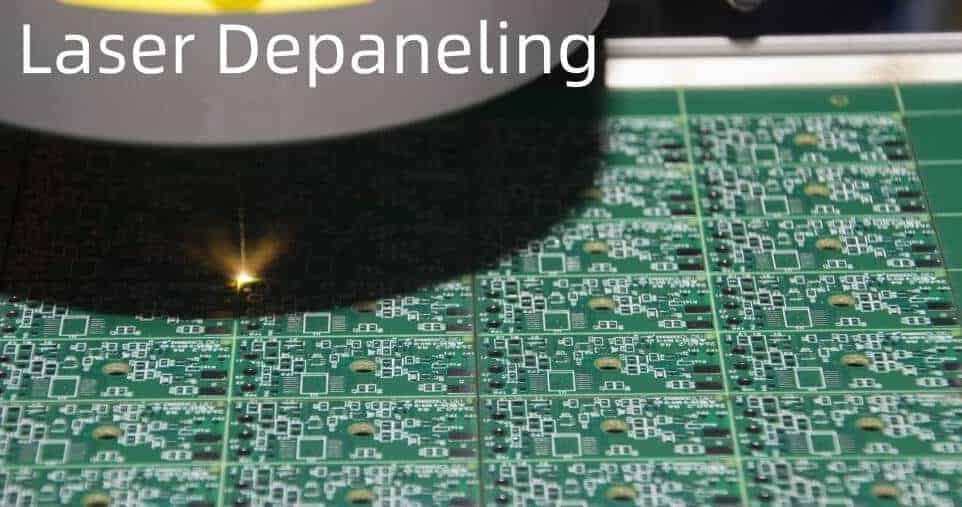
3. Laser Depaneling
Laser depaneling represents the cutting edge of PCB separation technology. UV lasers (typically 355nm wavelength) ablate material layer by layer using a “cold” cutting process that minimizes thermal damage.
Ten years ago, laser depaneling was exotic—expensive equipment reserved for aerospace and medical applications. Today, the price-performance ratio has improved by roughly a factor of ten, making laser depaneling practical for an expanding range of applications. It’s no longer a question of “if” laser will dominate high-end depaneling, but “when.”
A focused UV laser beam vaporizes PCB material in a controlled path. The laser makes multiple passes, removing material layer by layer until complete separation. Unlike CO2 lasers (which cut via thermal melting), UV lasers operate at a wavelength that breaks molecular bonds directly—a process called ablation. This is why UV laser cutting is often called “cold” cutting, even though localized heat is still generated.
Key advantages include:
No physical contact = zero mechanical stress on components
Kerf width under 25μm = maximum material utilization (fit more boards per panel)
CAD-driven paths = instant design changes without tooling modifications
Consistent quality = no tool wear means the 10,000th cut is identical to the first
The cutting speed depends on material type and thickness. For a standard 1.0mm FR-4 board, expect approximately 10-30 mm/s effective cutting speed. Thicker boards require more passes and proportionally longer cycle times. Flex circuits, on the other hand, cut remarkably fast.
Laser Depaneling Specifications
Parameter
Typical Value
Laser wavelength
355nm (UV)
Kerf width
15μm – 50μm
Heat-affected zone (HAZ)
<100μm
Positional accuracy
±4μm
Component clearance
As close as 100μm
When to Use Laser Depaneling
Laser is ideal for HDI boards, flex circuits, and any application where mechanical stress is unacceptable. It’s particularly valuable for medical devices, aerospace electronics, and high-reliability applications.
Pros:
Zero mechanical stress
Smallest kerf width = more boards per panel
Cuts any shape including complex curves
No tool wear or replacement
Handles flex and rigid-flex circuits
Cons:
Higher equipment cost
Slower for thick boards (>1.6mm)
Initial setup and programming required
Requires fume extraction
4. Punching (Die Cutting) Depaneling
Punching uses a custom-designed die to stamp individual PCBs out of the panel in a single press stroke. It’s one of the fastest methods for high-volume production of simple board shapes.
How Punching Works
A two-part fixture consists of:
Upper die with sharp cutting blades
Lower die with supports matching the PCB outline
The panel is positioned between dies, and a press forces the upper die down, shearing the connecting material and releasing individual boards.
Punching Specifications
Parameter
Typical Value
Cycle time
1-3 seconds per press
Die cost
$2,000 – $10,000+ (custom per design)
Stress level
Moderate to high
Board complexity
Simple shapes only
Volume suitability
High volume (>10,000 units)
When to Use Punching
Punching makes economic sense only for high-volume production where the die tooling cost can be amortized. It’s common in consumer electronics manufacturing.
Pros:
Extremely fast cycle times
Consistent results across large volumes
Low per-unit cost at high volumes
Cons:
High tooling cost (new die for each design)
Dies require regular sharpening
Significant mechanical stress on boards
Limited to simple shapes
Not economical for low volumes
5. Saw (Blade) Depaneling
Saw depaneling uses a rotating diamond or carbide blade to cut through PCB panels in straight lines. It’s similar to a table saw but optimized for PCB materials.
How Saw Depaneling Works
The PCB panel is secured on a precision table and fed through a high-speed rotating blade. Saws can cut:
V-grooved panels (completing the cut)
Non-grooved panels (full-thickness cutting)
Saw Depaneling Specifications
Parameter
Typical Value
Blade diameter
50mm – 150mm
Blade thickness
0.3mm – 1.0mm
Cut speed
Up to 300mm/s
Cut type
Straight lines only
Dust generation
Low to moderate
When to Use Saw Depaneling
Sawing is fast and works well for thick panels or aluminum-substrate PCBs (MCPCBs) used in LED applications. However, it’s limited to straight cuts.
Pros:
Very fast for straight cuts
Handles thick boards and metal substrates
Lower dust generation than routing
Works on non-V-grooved panels
Cons:
Straight cuts only
Higher mechanical stress than routing
Blade wear requires replacement
Not suitable for complex shapes
6. Manual Break (Hand Break) Depaneling
The simplest method: an operator manually snaps boards apart along V-grooves or perforated tab lines. No equipment required beyond possibly a simple fixture.
How Manual Break Works
The operator:
Positions the panel in a support fixture
Applies bending force along the V-groove or tab line
Snaps boards apart
Some facilities use a manual “pizza cutter” style tool that rolls along V-grooves to assist separation.
When to Use Manual Break
Manual breaking is only appropriate for prototypes, very low volumes, or boards with no sensitive components near separation lines.
Pros:
Zero equipment cost
Immediate—no setup required
Flexible for any panel design with V-grooves
Cons:
High mechanical stress (highest of all methods)
Inconsistent quality
Risk of board damage and component cracking
Operator-dependent results
Not suitable for production volumes
7. Water Jet Depaneling
Water jet cutting uses a high-pressure stream of water (often mixed with abrasive particles) to cut through PCB material. While less common than other methods, it has niche applications.
How Water Jet Works
Water at 30,000–90,000 PSI is forced through a tiny orifice (0.1–0.5mm), creating a cutting stream that can slice through most materials including FR-4, aluminum, and even metal-core PCBs.
When to Use Water Jet
Water jet is primarily used for prototype work or specialized applications where other methods aren’t suitable. The need for drying and potential water ingress limits its use for assembled boards.
Pros:
Cuts virtually any material
No heat-affected zone
Excellent edge quality
Cons:
Boards require thorough drying
Water exposure risk for sensitive components
Slower than most alternatives
Higher operating cost
Limited adoption in electronics manufacturing
PCB Depaneling Method Comparison Table
Here’s a side-by-side comparison to help you choose the right method:
Method
Stress Level
Speed
Cost
Shape Flexibility
Best For
V-Cut
Medium
Fast
Low
Straight only
High-volume rectangular boards
Router
Low
Medium
Medium
High
Complex shapes, sensitive components
Laser
None
Medium-Slow
High
Highest
Flex PCBs, HDI, medical/aerospace
Punching
High
Very Fast
High (tooling)
Low
Ultra-high volume simple boards
Saw
Medium-High
Fast
Medium
Straight only
Thick boards, metal-core PCBs
Manual
Very High
Slow
Very Low
Limited
Prototypes only
Water Jet
Low
Slow
High
High
Special materials, prototypes
How to Choose the Right PCB Depaneling Method
Selecting the optimal depaneling method depends on several factors. Here’s a practical decision framework that covers the key considerations:
Consider Your Board Design
Your board geometry is often the first filter in narrowing down options:
Rectangular with straight edges? → V-Cut or Saw (fastest, most economical)
Complex shapes or curves? → Router or Laser (only options for non-linear cuts)
Flex or rigid-flex? → Laser (mechanical methods risk substrate damage)
Very thin (<1.0mm)? → Router or Laser (V-Cut creates instability)
Thick (>2.5mm)? → Saw or Router (laser becomes slow, V-Cut difficult to break)
Metal-core (MCPCB)? → Saw (designed for hard substrates)
Consider Your Components
Component sensitivity often drives the depaneling decision more than any other factor:
Sensitive to mechanical stress? → Laser or Router (minimal induced strain)
Components near edges (<1mm)? → Laser (only method with ultra-low clearance)
Heavy components? → Avoid V-Cut (board flexing during separation risks cracked joints)
BGA or fine-pitch components? → Minimize stress—Router or Laser
Ceramic chip capacitors near edges? → Router or Laser (ceramics are crack-sensitive)
Tall components near separation lines? → Router (can navigate around height, unlike V-Cut machines)
Consider Your Volume
Different volumes have different economic sweet spots:
Prototype (<100 units) → Manual or Router (no tooling investment justified)
Based on years of production experience, here are the practices that consistently deliver better results:
Design-Stage Considerations
The most important decisions affecting depaneling quality happen long before boards reach the separation machine. Getting these right saves countless headaches later:
Plan depaneling during PCB design—not after. The method you choose affects component placement, panel utilization, and even your BOM cost.
Maintain component clearance: minimum 1mm from V-grooves, 0.5mm from router paths. For BGA packages and other stress-sensitive components, consider 1.5-2mm clearance.
Orient components parallel to separation lines to minimize stress impact. SMD chip components are particularly vulnerable to cracks when oriented perpendicular to cut lines.
Add fiducials for vision-guided systems. At least two per board, positioned diagonally opposite from each other.
Consider edge rail width for handling during depaneling. A 5mm rail provides enough material for clamping without wasting excessive panel space.
Communicate with your manufacturer early. They may have specific requirements or recommendations based on their equipment capabilities.
Production Considerations
Once panels are in production, these practices maintain quality and throughput:
Use fixtures to support boards during separation—unsupported boards flex more and suffer greater stress.
Implement dust extraction for routing operations. FR-4 dust is hazardous and can contaminate nearby equipment.
Monitor tool wear and establish replacement schedules. A worn router bit or dull V-Cut blade causes dramatically higher board stress.
Validate first articles before production runs. Measure edge quality, check for micro-cracks, and verify dimensional accuracy.
Document settings for repeatability across operators and shifts. The same board cut with different machine parameters can yield very different stress levels.
Maintain environmental controls if using laser depaneling—temperature and humidity affect cutting consistency.
Quality Control
Post-depaneling inspection catches problems before they reach customers:
Visual inspection of edges for cracks, delamination, or burrs
Dimensional verification against tolerances (critical for boards going into enclosures)
Electrical testing post-depaneling for critical assemblies
Sample stress testing per IPC guidelines for high-reliability products
Statistical process control to track quality trends over time
Stress Comparison: What the Data Shows
Independent testing has quantified the stress levels from different depaneling methods. Here’s what matters for long-term product reliability:
Method
Typical Strain (με)
Risk Level
Recommended For
Laser
<50
Very Low
Class 3 applications
Router
150-300
Low
Sensitive components
V-Cut Separator
300-500
Medium
General production
Saw
400-600
Medium-High
Thick/metal boards
Punching
500-800
High
High-volume simple
Manual Break
800-1500+
Very High
Prototypes only
Key insight: Strain is always higher perpendicular to the cut direction. Mount chip components parallel to separation lines whenever possible. Ceramic capacitors are particularly vulnerable—they can develop internal cracks that cause failures weeks or months after production.
A study published in the SMT Journal measured solder joint stress during different depaneling methods. The findings were clear: manual breaking generated stress peaks over 1000 με (microstrain), while proper router depaneling stayed below 250 με. Laser depaneling? Essentially immeasurable.
IPC guidelines recommend keeping components at least 1mm from cutting lines for V-groove separation and as close as 0.1mm for laser cutting. These aren’t arbitrary numbers—they’re based on extensive testing of solder joint reliability under induced stress.
The Hidden Cost of High-Stress Depaneling
What makes stress-induced defects particularly insidious is that they often don’t show up immediately. A hairline crack in a ceramic capacitor or a stressed solder joint may pass all inspection and testing, only to fail in the field after thermal cycling. These field failures are expensive:
Warranty claims and replacements
Customer dissatisfaction and lost repeat business
Root cause analysis and process investigation
Potential liability issues for safety-critical products
For high-reliability products, the cost of low-stress depaneling (whether router or laser) is almost always justified by reduced field failure rates.
Useful Resources and Downloads
For engineers looking to dive deeper, these resources provide valuable technical guidance:
Industry Standards
IPC-2221 – Generic Standard on Printed Board Design (includes panelization guidelines)
IPC-6012 – Qualification and Performance Specification for Rigid Printed Boards
IPC-A-610 – Acceptability of Electronic Assemblies
IPC-TM-650 – Test Methods Manual
Design Tools
LPKF Panel Layout Optimization Tool – Calculate material savings for laser vs. router (laser-depaneling.lpkf.com)
Your PCB fabricator’s DFM guidelines – Always check manufacturer-specific requirements
Further Reading
Wikipedia: Depaneling – Good overview of methods
AllPCB Blog: Comprehensive Guide to PCB Depaneling
JLCPCB: V-Cut Panelization Standards
Frequently Asked Questions (FAQs)
What is the difference between V-Cut and mouse bites (stamp holes)?
V-Cut creates a continuous V-shaped groove across the entire panel, allowing boards to snap apart along a straight line. It produces clean edges but only works for straight cuts. Mouse bites (also called stamp holes or perforated tabs) are a series of small drilled holes along the separation line. They allow for more flexible board shapes and curved edges but leave rougher edges that may need sanding. Mouse bites generate lower stress during separation compared to V-Cut breaking.
Can laser depaneling damage components near the cut line?
No—when properly implemented, UV laser depaneling is the safest method for components near the cut line. The heat-affected zone (HAZ) is typically less than 100μm from the cut edge, and temperatures just 100μm away from the cutting channel remain far below levels that could damage components. This is why laser depaneling is preferred for high-density designs where components must be placed close to board edges.
What is the most cost-effective PCB depaneling method?
For most production scenarios, V-Cut depaneling offers the best cost-per-board. It requires minimal equipment investment, has fast cycle times, and produces no kerf waste (maximum material utilization). However, the “most cost-effective” answer depends on your specific situation. For complex shapes, the added material utilization from laser cutting (due to tiny kerf widths) may offset higher equipment costs. For very high volumes of simple boards, punching can achieve the lowest per-unit cost despite expensive tooling.
How close can components be placed to depaneling lines?
This depends entirely on your depaneling method:
Method
Minimum Component Clearance
Manual break
3-5mm recommended
V-Cut machine
1.0mm minimum
Router
0.5mm minimum
Laser
0.1mm (100μm) possible
Always consult your depaneling equipment specifications and run test panels to validate clearances for your specific design.
Does depaneling method affect PCB reliability?
Yes—the mechanical stress induced during depaneling can affect long-term reliability. High-stress methods (manual breaking, aggressive punching) can create micro-cracks in solder joints that may not cause immediate failures but lead to field returns over time. For IPC Class 3 products (high-reliability applications like medical devices, aerospace, and automotive), low-stress methods like laser or router depaneling are strongly recommended. Testing per IPC-TM-650 can verify that your chosen method doesn’t compromise board reliability.
Conclusion
Choosing the right PCB depaneling method isn’t just about cost or speed—it’s about matching the technique to your specific board design, component sensitivity, volume requirements, and quality standards.
For most rectangular boards in medium-to-high volumes, V-Cut remains the reliable workhorse. It’s fast, economical, and produces clean edges when properly implemented. When you need shape flexibility and low stress, router depaneling delivers excellent results and adapts quickly to design changes. For the most demanding applications—flex circuits, HDI boards, or medical devices—laser depaneling eliminates mechanical stress entirely and provides the precision that modern miniaturized electronics require.
The industry trend is clear: as components get smaller and boards get denser, the tolerance for depaneling-induced stress decreases. Methods that worked fine ten years ago may cause unacceptable failure rates with today’s 0201 components and ultra-fine pitch BGAs. Smart manufacturers are investing in lower-stress methods proactively, rather than waiting for quality problems to force their hand.
The best approach? Consider depaneling requirements during your PCB design phase, talk to your assembly partner early, and don’t be afraid to request stress testing data for critical applications. The few hours invested upfront can save weeks of troubleshooting field failures later.
If you’re starting a new project, take the time to understand your options. Talk to equipment suppliers, request sample cuts on your specific board design, and measure the results. The right depaneling method, properly implemented, is invisible—your boards simply work, your customers are happy, and your production line runs smoothly. That’s the goal we’re all working toward.
Inquire: Call 0086-755-23203480, or reach out via the form below/your sales contact to discuss our design, manufacturing, and assembly capabilities.
Quote: Email your PCB files to Sales@pcbsync.com (Preferred for large files) or submit online. We will contact you promptly. Please ensure your email is correct.
Notes: For PCB fabrication, we require PCB design file in Gerber RS-274X format (most preferred), *.PCB/DDB (Protel, inform your program version) format or *.BRD (Eagle) format. For PCB assembly, we require PCB design file in above mentioned format, drilling file and BOM. Click to download BOM template To avoid file missing, please include all files into one folder and compress it into .zip or .rar format.


