Inquire: Call 0086-755-23203480, or reach out via the form below/your sales contact to discuss our design, manufacturing, and assembly capabilities.
Quote: Email your PCB files to Sales@pcbsync.com (Preferred for large files) or submit online. We will contact you promptly. Please ensure your email is correct.
Notes: For PCB fabrication, we require PCB design file in Gerber RS-274X format (most preferred), *.PCB/DDB (Protel, inform your program version) format or *.BRD (Eagle) format. For PCB assembly, we require PCB design file in above mentioned format, drilling file and BOM. Click to download BOM template To avoid file missing, please include all files into one folder and compress it into .zip or .rar format.
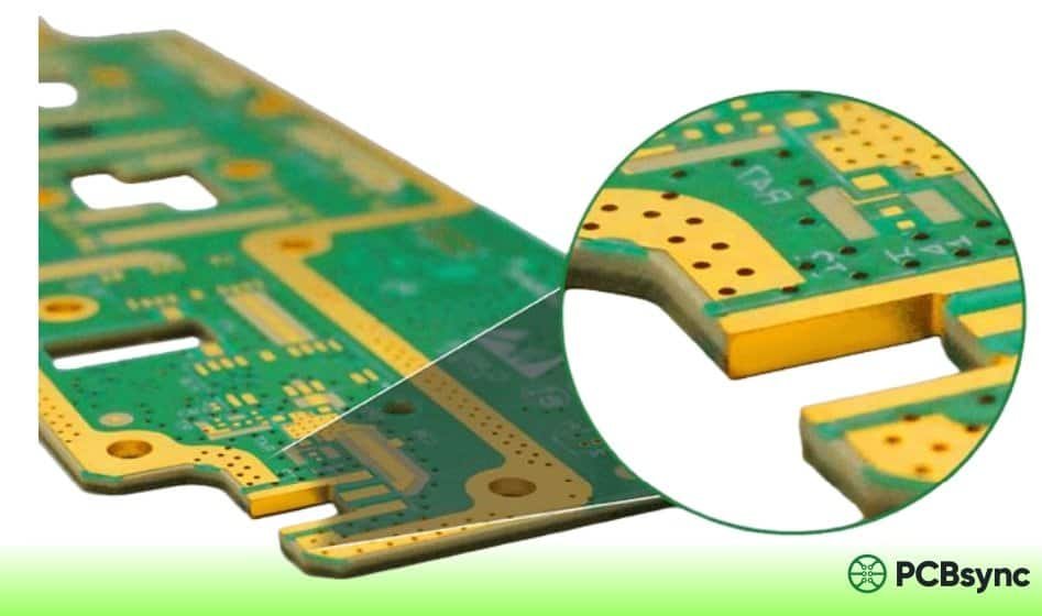
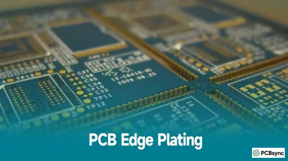
If you’ve worked on RF designs, high-speed boards, or anything that needs solid EMI shielding, you’ve probably come across PCB edge plating. It’s one of those techniques that sounds simple on paper—just plate the edges of your board with copper—but getting it right takes some know-how. I’ve seen plenty of designs come back from fab with peeling copper or short circuits because the design rules weren’t followed properly.
In this guide, I’ll walk you through everything you need to know about PCB edge plating: what it is, when you actually need it, the design rules that’ll save you from costly respins, and the manufacturing considerations that make or break your boards. Whether you’re designing your first edge-plated board or looking to troubleshoot an existing design, this should cover the practical stuff you need.
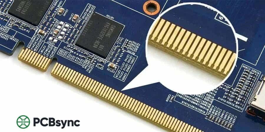
PCB edge plating—also called side plating, castellation, or metalized edge plating—is the process of applying a metallic coating along the perimeter edges of a circuit board. The copper plating runs from the top surface to the bottom surface, creating a continuous conductive path along one or more edges of the board.
Unlike standard through-hole plating where you’re connecting internal layers through drilled holes, edge plating focuses on the board’s exterior. The process happens during the standard plating phase of PCB fabrication, but it requires routing the board profile before metallization—which is why V-cut scoring doesn’t work on edge-plated boards.
The typical surface finish for edge plating is ENIG (Electroless Nickel Immersion Gold), though you can also use immersion silver or other finishes depending on your application requirements.
Types of PCB Edge Plating
There are several ways to implement edge plating depending on your pcb design needs:
Single-axis plating: Plating applied to one edge only. Common for boards that slide into metal enclosures or need grounding on one side.
Multi-axis plating: Plating on two or more edges. Often used for RF shielding where you need more complete coverage.
Full perimeter plating: All four edges plated. Provides maximum EMI shielding but requires tabs (unplated segments) for panel support during PCB manufacturing.
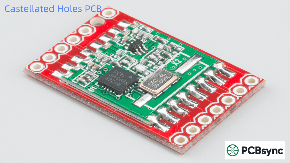
Castellated holes: Half-circle plated holes along the board edge. Used for module-to-motherboard connections in surface-mount applications.
Why Use PCB Edge Plating? Key Benefits
Edge plating isn’t just for show—it solves real engineering problems. Here’s when it makes sense to specify it:
EMI Shielding and Containment
This is the big one. In high-frequency designs operating in the megahertz to gigahertz range, the board edges can radiate electromagnetic interference. Edge plating creates a conductive shield around the perimeter, essentially forming a partial Faraday cage that contains electromagnetic fields.
For RF applications—think Wi-Fi modules, Bluetooth devices, or anything operating above a few hundred MHz—this can be the difference between passing and failing EMC testing. I’ve seen edge plating help boards pass radiated emissions tests that were previously failing by 6-8 dB.
Improved Grounding
Edge plating provides a direct, low-impedance path to ground. When your board mounts in a metal enclosure, the plated edges make solid contact with the chassis, creating a continuous ground reference. This is particularly important for high-speed digital signals where even small ground discontinuities can cause signal integrity problems.
Thermal Management
The metallized edges create additional surface area for heat dissipation. When connected to internal ground planes through thermal vias, edge plating can provide a significant thermal path to the enclosure. In automotive power modules, for example, this can reduce hot-spot temperatures by 5-10°C.
Mechanical Protection
Exposed board edges are vulnerable to delamination and damage during handling. The copper plating reinforces the edge, protecting against mechanical stress and environmental factors like moisture ingress. This matters in aerospace and industrial applications where boards face repeated handling or harsh conditions.
Benefits Summary
Benefit
Application
EMI Shielding
RF modules, wireless devices, high-speed digital circuits
Grounding
Chassis-mounted boards, shielded enclosures, LVDS systems
Thermal Management
Power electronics, LED drivers, automotive modules
Getting edge plating right starts in your CAD tool. Here are the design rules you need to follow—skip these and you’ll either get DFM feedback from your fab house or, worse, boards that fail in production.
Copper Overlap Requirements
To guarantee manufacturability, you need overlapping copper in your layout file to define where edge plating should be applied. The copper pour should extend past the board edge—this gives the plating something to adhere to.
Critical Dimensions
Parameter
Value
Minimum copper overlap (over board edge)
0.5 mm (500 μm)
Minimum connected copper (on connected layers)
0.3 mm (300 μm)
Minimum gap on non-connected layers
0.8 mm (800 μm)
Clearance to different-net copper
0.25 mm (10 mils)
Clearance between plated edge sections
2.5 mm (100 mils)
Minimum component clearance from plated edge
0.5 mm
Minimum corner radius
0.3 mm
Recommended board thickness
≥1.6 mm
Panel Support Tab Requirements
Here’s something that catches people off guard: if you’re plating all four edges, you can’t plate 100% of the perimeter. The fab house needs to hold your boards during manufacturing, which means leaving 3-4 short unplated segments (at least 3mm spacing) for panel support tabs.
Place these tabs in non-critical areas where a small gap in shielding won’t matter. If you don’t specify tab locations, the fabricator will choose them—and they might not pick the spots you’d prefer.
Power Plane Clearance
Critical: Never let internal power planes extend to the board edge where plating will be applied. If a power plane contacts the edge plating, you’ll short it to ground. Always maintain clearance between internal power layers and the plated edge—most designers use the ground plane setback rules from their fab house, typically 0.5-1mm.
How to Specify Edge Plating in Your CAD Tool
The implementation varies by software, but the general approach is the same:
Define the edge plating using a polygon pour that extends over the board edge by at least 0.5mm
Assign the edge plating to a net—typically ground for EMI shielding applications
Set a negative board outline clearance rule (in Altium, for example) to allow the pour to extend past the board edge
Add clear notation in your fabrication drawing specifying which edges need plating and the required thickness
Manufacturing Process and Considerations
Understanding how edge plating is manufactured helps you design boards that fabricators can actually build reliably.
The Edge Plating Process Flow
Edge plating happens during the standard PCB plating phase, but with a key difference: the board profile where plating is needed must be routed before metallization. Here’s the typical sequence:
Drilling and routing of the board profile (where edge plating is required)
Edge preparation: cleaning, degreasing, and surface roughening for adhesion
Copper deposition via electroplating (typically 25-50 μm thickness)
Final routing to remove support tabs and separate boards
Because routing happens before plating, V-cut scoring isn’t compatible with edge plating. The board edges need to be fully separated before the copper goes down.
For most edge plating applications, ENIG is the recommended choice. It provides excellent corrosion resistance and maintains consistent electrical properties over time.
Common Challenges and Solutions
Copper Peeling: Plating over large substrate areas can lead to adhesion failures. The solution is proper edge preparation—roughening the surface through chemical and mechanical means before plating.
Burrs: The final routing process can create burrs on castellated holes or plated edges. Quality fabricators use modified process flows that polish burrs down to the feature edge.
Incomplete Coverage: Misaligned routing or insufficient copper overlap leads to gaps in plating. Clear fabrication drawings and manufacturer communication prevent this.
Short Circuits: Power planes too close to plated edges will short to ground. Always verify clearances during DRC and in your fabrication notes.
Quality Control and Inspection
When your boards come back, here’s what to check:
Plating Thickness: Verify minimum thickness (typically 25-50 μm) via microsection or X-ray fluorescence. Thin plating leads to wear and corrosion issues.
Continuity Testing: Confirm electrical connectivity from internal layers through the plated edge contacts. Use a multimeter to check resistance—it should be less than 1 milliohm per square centimeter.
Visual Inspection: Look for voids, cracks, or uneven coverage. Pay attention to corners where plating tends to be thinner.
Adhesion Testing: For critical applications, tape tests can verify the plating won’t peel under mechanical stress.
How to Order Edge-Plated PCBs
Communication with your fabricator is critical. Here’s what to include in your order:
Annotated diagram clearly showing which edges require plating
Surface finish specification for the plated edges
Required copper thickness (if different from standard)
Tab locations if you have preferences for panel support placement
Which internal layers (if any) should connect to the edge plating
In your fabrication notes, include something like: “Plate edges circled in red per attached diagram. Surface finish: ENIG. Connect to ground planes on layers 1 and 4.”
Useful Resources
Here are some resources that can help you design and specify edge plating correctly:
Industry Standards
IPC-6012: Qualification and Performance Specification for Rigid PCBs—includes edge plating requirements
IPC-A-600: Acceptability of Printed Boards—defines visual criteria for plated edges
IPC-2221: Generic Standard on PCB Design—includes edge plating design guidelines
1. What is the difference between edge plating and castellated holes?
Edge plating covers continuous sections of the board perimeter with copper. Castellated holes (also called castellations) are half-circle plated holes cut along the edge, typically used for surface-mount module connections. Both involve plating on the board edge, but castellations provide discrete connection points while edge plating creates continuous shielding or grounding surfaces.
2. Can I use V-scoring on edge-plated boards?
No. V-cut scoring requires the board profile to remain intact during plating, but edge plating requires routing the profile before metallization. These processes are incompatible. If you need edge plating, you’ll have to use tab routing for depanelization instead of V-scoring.
3. How much does edge plating add to PCB cost?
Edge plating typically adds 10-20% to the board fabrication cost, depending on the number of edges plated and the surface finish selected. The main cost drivers are the additional routing before plating, the plating material itself, and the more careful handling required. For high-volume production, negotiate with your fabricator—the premium decreases significantly at scale.
4. Which surface finish is best for edge plating?
ENIG (Electroless Nickel Immersion Gold) is the most commonly recommended finish for edge plating. It provides excellent oxidation resistance, maintains consistent electrical properties, and has good durability. For applications requiring thousands of mating cycles (like edge connectors), hard gold is better but significantly more expensive. Immersion silver works for cost-sensitive applications but has a shorter shelf life.
5. Can edge plating cause short circuits with internal power planes?
Yes, this is a real risk if not designed correctly. The edge plating is typically connected to ground, so any power plane that extends to the board edge will be shorted. Always maintain adequate clearance between internal power layers and plated edges—typically 0.5-1mm minimum. Most EDA tools can enforce this with design rules. Review your layer stackup carefully before sending boards to fab.
Conclusion
PCB edge plating is a straightforward technique that solves real engineering problems—EMI containment, improved grounding, thermal management, and mechanical protection. The key to success is following the design rules: proper copper overlap, adequate clearances, and clear communication with your fabricator.
If you’re designing RF boards, high-speed digital systems, or anything that needs to mount in a shielded enclosure, edge plating is worth considering. The modest cost increase is usually justified by the performance benefits and reduced EMC testing headaches.
Start with the design rules in this guide, confirm capabilities with your fab house before finalizing your layout, and always include clear fabrication notes. Get those fundamentals right, and edge plating becomes just another reliable tool in your PCB design toolkit.
Inquire: Call 0086-755-23203480, or reach out via the form below/your sales contact to discuss our design, manufacturing, and assembly capabilities.
Quote: Email your PCB files to Sales@pcbsync.com (Preferred for large files) or submit online. We will contact you promptly. Please ensure your email is correct.
Notes: For PCB fabrication, we require PCB design file in Gerber RS-274X format (most preferred), *.PCB/DDB (Protel, inform your program version) format or *.BRD (Eagle) format. For PCB assembly, we require PCB design file in above mentioned format, drilling file and BOM. Click to download BOM template To avoid file missing, please include all files into one folder and compress it into .zip or .rar format.


