Inquire: Call 0086-755-23203480, or reach out via the form below/your sales contact to discuss our design, manufacturing, and assembly capabilities.
Quote: Email your PCB files to Sales@pcbsync.com (Preferred for large files) or submit online. We will contact you promptly. Please ensure your email is correct.
Notes: For PCB fabrication, we require PCB design file in Gerber RS-274X format (most preferred), *.PCB/DDB (Protel, inform your program version) format or *.BRD (Eagle) format. For PCB assembly, we require PCB design file in above mentioned format, drilling file and BOM. Click to download BOM template To avoid file missing, please include all files into one folder and compress it into .zip or .rar format.
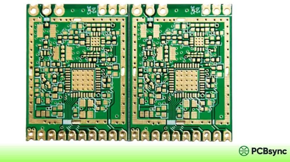
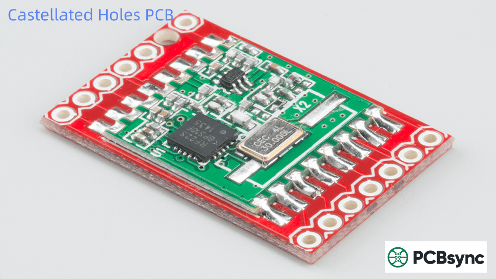
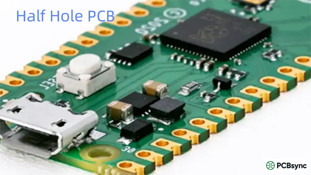
If you’ve worked with WiFi modules, Bluetooth boards, or any compact electronic module, you’ve probably noticed those distinctive half-moon shaped holes running along the edges. These are castellated holes PCB features—also called plated half-holes or half hole PCBs—and they’ve become essential in modern electronics design.
I’ve been designing PCBs for over a decade, and castellated holes PCB technology has genuinely changed how we approach modular design. Instead of dealing with bulky connectors and complex wiring harnesses, we can now solder one board directly onto another. The result? Thinner products, fewer failure points, and simpler assembly processes.
This guide covers everything you need to know about castellated holes PCB design, from basic concepts to advanced manufacturing considerations. Whether you’re designing your first castellated module or optimizing an existing design, you’ll find practical specifications and real-world tips that work.
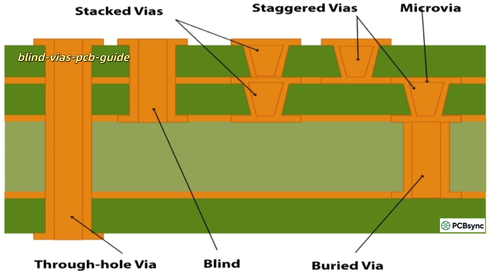
A castellated holes PCB features plated semi-circular holes along its board edges. These holes are created by drilling standard plated through-holes, then cutting the board directly through those holes during the profiling process. What remains is a row of half-circle, copper-plated indentations that serve as both electrical connections and mechanical mounting points.
The name “castellated” comes from their resemblance to castle battlements—those notched defensive walls you see in medieval architecture. In the PCB industry, you’ll hear these called castellated holes, plated half-holes, edge-plated holes, or simply half holes. They all refer to the same feature.
The fundamental purpose is straightforward: enabling board-to-board connections without connectors. When you solder a castellated holes PCB module onto a carrier board, the half holes align with corresponding pads, creating permanent electrical and mechanical bonds.
Castellated Holes PCB vs Traditional Through-Hole Technology
Understanding when to use castellated holes PCB versus traditional approaches helps you make better design decisions.
Castellated holes PCB designs shine when you need compact, permanent connections. They’re not ideal when you need to frequently disconnect modules or when you’re prototyping and expect many board revisions.
Why Use Castellated Holes PCB Design?
The practical benefits of castellated holes PCB technology extend across design, manufacturing, and product performance.
Space Efficiency
Traditional connectors add significant height and footprint to your assembly. A standard 2.54mm pin header with mating socket adds roughly 8-11mm of vertical clearance. Castellated holes PCB mounting eliminates this entirely—your module sits flush against the carrier board.
For products like wearables, medical implants, or ultra-thin consumer electronics, this matters enormously. I’ve seen designs where switching to castellated modules reduced overall product thickness by 40% or more.
Improved Reliability
Connectors fail. Pins corrode, sockets wear out, and vibration loosens connections over time. Castellated holes PCB joints are permanent solder connections with no mechanical wear surfaces.
In high-vibration environments—automotive electronics, industrial equipment, drones—this reliability difference is critical. The soldered castellated connection distributes stress across the entire joint rather than concentrating it at individual pin contacts.
Lower Assembly Costs
No connectors means no connector costs. Beyond the component savings, you eliminate connector placement operations during assembly. For high-volume production, this adds up quickly.
The reflow soldering process for castellated holes PCB modules integrates with standard SMT assembly lines. No separate through-hole insertion steps, no wave soldering operations, no manual header installation.
Better Signal Integrity
Shorter signal paths mean less inductance and capacitance. When you solder a module directly to a carrier board, the connection path is essentially the thickness of the solder joint—typically under 0.5mm.
For high-frequency applications like WiFi modules operating at 2.4GHz or 5GHz, this matters. Board-to-board connectors can introduce measurable impedance discontinuities. Direct castellated holes PCB connections minimize these effects.
Cleaner Design
Castellated holes PCB connections create a sealed interface between boards. Dust, moisture, and contaminants can’t easily infiltrate the joint area like they can with open pin headers. For products used in harsh environments, this inherent sealing provides meaningful protection.
Getting specifications right prevents manufacturing problems and ensures reliable connections. These numbers come from actual production experience across multiple fabrication houses.
Hole Positioning: Place the hole center exactly on the board outline. Not inside the outline, not outside—exactly on it. Your CAD software should show half the hole on the board, half outside. If the center is offset inward, you won’t get a proper castellated hole. If it’s offset outward, you’ll have manufacturing problems.
Pad Coverage: Every castellated hole needs a pad on each copper layer it touches. For a 4-layer board, that means pads on top, bottom, and both inner layers. The pads must fully surround the hole portion that remains on the board. Insufficient pad coverage leads to plating delamination.
Inner Layer Connections: When possible, connect inner layer pads to the plated holes. This adds mechanical stability and reduces the risk of burrs during milling. Some manufacturers require this for holes smaller than 0.6mm.
Solder Mask Openings: Create solder mask openings that expose the castellated hole plus surrounding pad. Standard practice is to open the mask 0.1-0.15mm beyond the pad edge. This ensures proper solder wetting during assembly.
Right-Angle Castellated Holes: If you need castellated holes at board corners (90-degree positions), use larger hole diameters—typically 1.2mm minimum. Corner positions experience more stress during milling and are prone to damage with smaller holes.
Surface Finish Recommendations for Castellated Holes PCB
Surface finish choice significantly impacts castellated hole quality and solderability.
ENIG (Electroless Nickel Immersion Gold) is the standard recommendation for castellated holes PCB designs. The flat, consistent plating works well with the castellated hole geometry. Avoid HASL (Hot Air Solder Leveling) for small-diameter castellated holes—the uneven solder coating can partially fill or block the holes.
Castellated Holes PCB Manufacturing Process
Understanding the manufacturing process helps you design boards that fabricate cleanly and avoid common production issues.
Step-by-Step Manufacturing Flow
1. Standard PCB Fabrication: The board goes through normal fabrication steps—lamination, imaging, etching—until the drilling stage.
2. Drilling: Full circular holes are drilled at the edge positions where castellated holes are required. These are drilled as standard plated through-holes, not as edge features yet.
3. Copper Plating: Electroless copper followed by electrolytic copper plates the hole walls. The plating thickness needs to meet specifications (typically 25µm minimum) because only half this plating will remain after cutting.
4. Remaining Fabrication: Outer layer imaging, etching, solder mask, and surface finish proceed as normal.
5. Profile Milling: Here’s where castellated holes are created. A CNC milling machine cuts the board outline directly through the center of the plated holes. This is the critical step.
6. Deburring and Inspection: After milling, technicians inspect and deburr the castellated holes. Copper burrs inside the holes can cause shorts or weak solder joints.
Castellated Holes PCB Manufacturing Challenges and Quality Issues
Copper Burrs: The most common defect in castellated holes PCB production. When the milling tool cuts through the copper barrel, it can pull or tear the copper rather than cutting cleanly. Burrs inside castellated holes prevent proper solder flow and can cause shorts between adjacent holes.
Quality manufacturers use heavy-duty carbide milling bits and carefully controlled cutting speeds. Some use specialized tooling designed specifically for castellated hole profiling.
Plating Delamination: If the copper plating isn’t properly bonded to the hole wall, the milling operation can lift or peel the plating. This usually indicates process problems during electroless copper deposition or inadequate surface preparation.
Dimensional Tolerance: The milling process must cut exactly through the hole center. If the routing path is off by even 0.1mm, you get asymmetric castellated holes that don’t align properly with carrier board pads.
Hole Wall Damage: Aggressive milling parameters can damage the remaining half of the hole wall, leaving rough surfaces that don’t wet properly during soldering.
Selecting a Manufacturer for Castellated Holes PCB
Not all PCB fabricators handle castellated holes equally well. When evaluating manufacturers for castellated holes PCB projects, consider:
Minimum castellated hole diameter capability (0.4mm vs 0.6mm indicates process sophistication)
Deburring and inspection procedures
Experience with your board thickness and layer count
Sample boards or references from similar projects
For prototypes, most major quick-turn fabricators (JLCPCB, PCBWay, etc.) offer castellated hole capability with reasonable quality. For production volumes, verify the manufacturer’s process control and quality metrics specifically for castellated hole features.
How to Design Castellated Holes in Popular CAD Software
The actual CAD implementation of castellated holes is simpler than you might expect. The key principle is the same across all tools: place standard plated through-holes on the board outline, then let the manufacturing process create the castellated holes.
General Design Approach for Castellated Holes PCB
Draw your board outline normally
Place plated through-hole pads at edge locations where you want castellated holes
Position each hole so its center sits exactly on the board outline
Verify pads exist on all required layers
Include castellated holes in your plated drill file
Add a PCB manufacturing note specifying “castellated holes” or “plated half holes”
KiCad Implementation for Castellated Holes PCB
In KiCad, the most straightforward approach is creating through-hole pads on the board edge:
Create a new footprint for your castellated edge
Add through-hole pads with your required diameter
Position pads so their centers align with the Edge.Cuts layer
The pad will extend beyond the edge—this is correct
When you generate Gerbers, the drill file includes these holes as plated through-holes
Add text on a documentation layer: “Castellated holes required on this edge”
Altium Designer Implementation for Castellated Holes PCB
Altium handles castellated holes similarly:
Place standard pads with hole size matching your castellated hole requirement
Position pad centers on the board outline
Ensure pads are defined on all copper layers
In the drill file settings, these will export as plated through-holes
Add a mechanical layer note about castellated holes
The Altium pad properties should show the hole type as “Plated” and shape as “Round.” The overhang beyond the board edge is expected and handled during fabrication.
Design File Checklist for Castellated Holes PCB Manufacturers
When submitting files for boards with castellated holes, include:
Gerber files with all copper layers showing castellated hole pads
Drill file with castellated holes marked as plated through-holes (not NPTH)
Board outline on mechanical/edge layer
Clear documentation noting which edges have castellated holes
Specific castellated hole diameter and quantity
Any special requirements (surface finish, plating thickness)
Explicitly calling out castellated holes in your order notes prevents confusion. Some fabricators charge extra for castellated features, so specifying them upfront ensures accurate pricing.
Castellated Holes PCB Applications
Castellated holes PCB technology appears across virtually every electronics sector. Here are the primary application categories.
Wireless Communication Modules
This is the dominant use case for castellated holes PCB. WiFi modules like the ESP32-WROOM, Bluetooth modules, LoRa transceivers, and cellular modems almost universally use castellated mounting. The module manufacturer designs, certifies, and tests the complete RF system on a small PCB with castellated holes. End product designers simply solder this module onto their carrier boards without needing RF design expertise.
Popular wireless modules using castellated holes PCB design:
ESP32-WROOM-32 (WiFi + Bluetooth)
ESP8266 modules
HC-05/HC-06 Bluetooth modules
RFM95/96 LoRa modules
Nordic nRF52 modules
SIMCom cellular modules
Sensor Modules
Environmental sensors, IMUs, GPS receivers, and other sensor subsystems often come as castellated modules. This packaging protects sensitive components and provides known-good tested units for integration.
Development and Breakout Boards
The Raspberry Pi Pico, Seeed XIAO series, and many other development boards use castellated edges. This dual-purpose design lets hobbyists use pin headers for prototyping, then production designs can solder the same module directly using the castellated holes.
Power Supply Modules
DC-DC converters, voltage regulators, and power management ICs increasingly appear as castellated modules. These integrate all the required inductors, capacitors, and control circuitry, then mount directly to the main board.
Industrial and Automotive Electronics
In applications requiring vibration resistance and long-term reliability, castellated holes PCB modules offer advantages over connector-based solutions. Industrial control systems, automotive ECUs, and aerospace electronics use castellated hole technology extensively.
Soldering Castellated Holes PCB Modules
Proper soldering technique ensures reliable connections. Both hand soldering and reflow methods work well with castellated holes.
Hand Soldering Process for Castellated Holes PCB
Equipment needed:
Temperature-controlled soldering iron (350-380°C typical)
Fine tip appropriate for your castellated hole pitch
Quality solder (0.5-0.8mm diameter works well)
Flux (liquid or paste)
Tweezers
Magnification for inspection
Procedure:
Preparation: Apply flux to the carrier board pads. Ensure both the castellated holes and pads are clean.
Positioning: Align the module on the carrier board. The castellated holes should sit centered over the corresponding pads.
Tack one corner: Heat a corner pad and castellated hole simultaneously. Apply a small amount of solder. This fixes the module position.
Verify alignment: Check that all castellated holes align with their pads. Adjust if necessary by reheating the tack joint.
Solder remaining connections: Work around the module, heating each pad/castellated hole junction and flowing solder into the joint. The concave shape of the castellated hole naturally draws solder into the connection.
Inspection: Check each joint for proper wetting. Solder should flow smoothly up the castellated hole walls and wet both the hole and the pad surface.
Reflow Soldering Process for Castellated Holes PCB
For production assembly of castellated holes PCB modules, reflow soldering is standard:
Apply solder paste to carrier board pads using stencil printing
Place modules using pick-and-place equipment
Reflow using standard temperature profile for your solder paste
The paste wicks up into the castellated holes during reflow, creating reliable joints
Stencil design tip: Use apertures slightly larger than the pad size for castellated hole positions. The castellations can accommodate more solder paste than flat SMD pads, and the extra paste improves joint quality.
Common Soldering Problems with Castellated Holes PCB
Problem
Cause
Solution
Insufficient wetting
Cold joint, flux burned off
Ensure adequate temperature, fresh flux
Solder bridges
Excessive solder, insufficient spacing
Reduce solder amount, check design spacing
Lifted plating
Manufacturing defect or overheating
Use quality boards, control temperature
Poor alignment
Module shifted during soldering
Tack properly, use fixtures for production
Voids in joint
Trapped flux gas, contamination
Proper flux activation, clean surfaces
Castellated Holes PCB Cost Factors
Castellated holes PCB boards cost more than standard PCBs. Understanding why helps you budget accurately and optimize designs for cost when possible.
Why Castellated Holes PCB Costs More
Additional processing steps: The milling operation requires extra machine time and specialized tooling.
Higher scrap rates: Castellated holes PCB boards have more potential failure modes during manufacturing. Defective holes mean scrapped boards.
Inspection requirements: Each castellated hole needs individual inspection for burrs and plating quality. This adds labor cost.
Smaller board sizes: Modules are typically small, meaning more individual pieces per panel, more handling, and more edge processing per square inch of board material.
Cost Optimization Strategies for Castellated Holes PCB
Use standard dimensions: Hole diameters of 0.6mm or 0.8mm are easier to manufacture than 0.4mm or 0.5mm minimums.
Maximize spacing: Castellated holes spaced at 1.0mm or greater edge-to-edge cost less than 0.5mm spacing designs.
Minimize castellated hole count: Every castellated hole adds inspection time. Use only what your design requires.
Choose appropriate surface finish: ENIG is preferred but costs more. Immersion silver may work for applications with shorter shelf life requirements.
Panel efficiently: Work with your manufacturer to optimize panelization. Consistent castellated hole edges across the panel improve yield.
Volume pricing: Like all PCB features, castellated holes PCB costs decrease significantly with volume. Prototype pricing is much higher per board than production quantities.
Troubleshooting Common Castellated Holes PCB Issues
Problems with castellated holes PCB boards usually trace back to design issues, manufacturing defects, or assembly errors.
Design-Related Problems
Castellated holes not forming: If your board arrives with full round holes on the edge, check your drill file. The holes may not have been positioned exactly on the board outline, so the milling operation missed them.
Inconsistent castellated hole shape: Some holes more than half, some less? Your board outline may not be accurate, or the manufacturer’s registration is off. This affects pad alignment during assembly.
Plating missing from inner layers: If castellated holes aren’t connecting to inner layer pads, verify your design includes pads on those layers and that the pads surround the holes properly.
Manufacturing Defects
Copper burrs: Small copper fragments inside the castellated holes. These cause assembly defects and potential shorts. Quality manufacturers deburr, but inspection is still warranted for critical applications.
Rough hole walls: Indicates aggressive milling or dull tooling. Rough walls don’t wet properly during soldering. Request replacement boards if severe.
Delaminated plating: Copper pulling away from the hole wall, especially at the cut edge. This is a fabrication process problem requiring manufacturer correction.
Assembly Issues
Weak solder joints: Often caused by insufficient heat or oxidized surfaces. Castellated holes require adequate dwell time for solder to flow properly into the cavity.
Module misalignment: Castellated holes have less self-centering than BGA balls. Use fixtures or careful hand placement to ensure alignment before soldering.
Solder wicking away from joint: Usually indicates insufficient flux or contaminated surfaces. Clean both mating surfaces before assembly.
IPC Standards for Castellated Holes PCB
Industry standards provide guidelines for castellated holes PCB design and acceptance criteria.
Relevant IPC Standards
IPC-2221: General PCB design standard. Provides baseline requirements for hole sizing, spacing, and pad design that apply to castellated holes.
IPC-6012: Qualification and performance specification for rigid PCBs. Class 2 and Class 3 requirements include plating thickness and hole quality criteria applicable to castellated holes.
IPC-7351: Land pattern standard. Provides guidelines for footprint design including castellated mounting patterns.
IPC-A-600: Acceptability of printed boards. Defines visual inspection criteria for plated holes including edge plating quality.
Class 2 vs Class 3 Requirements for Castellated Holes PCB
Requirement
IPC Class 2
IPC Class 3
Copper plating thickness
20µm minimum
25µm minimum
Barrel crack allowance
Some acceptable
None acceptable
Void allowance
Limited
Minimal to none
Annular ring breakout
90° max
None acceptable
Documentation requirements
Standard
Full traceability
For most consumer and commercial products, Class 2 is sufficient. Medical devices, aerospace, military, and automotive safety systems typically require Class 3 castellated holes PCB standards.
Frequently Asked Questions About Castellated Holes PCB
What is the minimum hole diameter for castellated holes PCB?
The absolute minimum at most manufacturers is 0.4mm finished diameter. However, 0.6mm is the practical minimum for reliable manufacturing with standard processes. Smaller diameters require advanced fabrication capabilities and increase cost. For designs without severe space constraints, 0.8mm provides the best balance of reliability and manufacturability.
Can I use castellated holes on flexible PCBs?
Yes, but with significant caveats. Flexible PCBs can accommodate castellated holes, but the flex material is more prone to plating adhesion problems than rigid FR4. The milling operation also requires modified parameters for flex substrates. Most importantly, the board-to-board connection you create with castellated holes on flex should be in a non-flexing zone of the circuit, as the solder joints cannot tolerate repeated bending.
How do I specify castellated holes when ordering PCBs?
When placing your order, select the “Castellated Holes” or “Plated Half Holes” option if available. Include a note specifying which edges have castellated holes and the hole count and diameter. In your Gerber files, the holes should appear as standard plated through-holes positioned on the board outline. Most manufacturers charge an additional fee for castellated holes PCB processing, which should appear in your quote once you specify this feature.
What causes copper burrs in castellated holes and how can they be prevented?
Copper burrs form when the milling tool tears rather than cleanly cuts through the copper barrel. Contributing factors include dull tooling, incorrect cutting speeds, inadequate board support, and thin copper plating. From a design perspective, you can reduce burr risk by using larger hole diameters (0.6mm+), connecting inner layer pads to the holes for additional support, and specifying ENIG surface finish which provides a harder surface. Manufacturing-side solutions include sharp carbide tooling, optimized feed rates, and thorough post-milling deburring.
Are castellated holes PCB designs suitable for high-frequency applications?
Yes, and they’re often preferred over connector-based alternatives for RF applications. The short, direct connection path of a soldered castellated hole joint introduces less parasitic inductance and capacitance than pin headers or board-to-board connectors. WiFi, Bluetooth, LoRa, and cellular modules operating at frequencies from hundreds of MHz to several GHz routinely use castellated holes PCB mounting. For best RF performance, ensure continuous ground plane connections through multiple castellated holes and maintain controlled impedance on traces leading to the castellated edge.
What’s the difference between castellated holes and plated half holes?
These terms refer to the same feature. “Castellated holes” is the more formal industry term, named after the castle-like appearance of the notched board edge. “Plated half holes” is a more descriptive term that explains the manufacturing process—full plated holes cut in half. You may also hear “edge-plated holes” or simply “half holes.” When ordering PCBs, any of these terms will be understood by manufacturers.
Can castellated holes PCB modules be reworked?
Yes, but rework is more challenging than with socketed modules. To remove a castellated module, you need to simultaneously heat all solder joints while lifting the module—typically requiring hot air rework equipment or specialized fixtures. The carrier board pads can usually survive one or two rework cycles if done carefully. For designs where frequent module replacement is expected, consider whether castellated mounting is the right choice.
Inquire: Call 0086-755-23203480, or reach out via the form below/your sales contact to discuss our design, manufacturing, and assembly capabilities.
Quote: Email your PCB files to Sales@pcbsync.com (Preferred for large files) or submit online. We will contact you promptly. Please ensure your email is correct.
Notes: For PCB fabrication, we require PCB design file in Gerber RS-274X format (most preferred), *.PCB/DDB (Protel, inform your program version) format or *.BRD (Eagle) format. For PCB assembly, we require PCB design file in above mentioned format, drilling file and BOM. Click to download BOM template To avoid file missing, please include all files into one folder and compress it into .zip or .rar format.


