Inquire: Call 0086-755-23203480, or reach out via the form below/your sales contact to discuss our design, manufacturing, and assembly capabilities.
Quote: Email your PCB files to Sales@pcbsync.com (Preferred for large files) or submit online. We will contact you promptly. Please ensure your email is correct.
Notes: For PCB fabrication, we require PCB design file in Gerber RS-274X format (most preferred), *.PCB/DDB (Protel, inform your program version) format or *.BRD (Eagle) format. For PCB assembly, we require PCB design file in above mentioned format, drilling file and BOM. Click to download BOM template To avoid file missing, please include all files into one folder and compress it into .zip or .rar format.
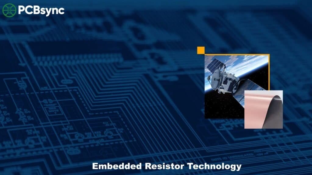
If you’ve spent any time designing high-speed circuits or RF boards, you’ve probably hit the wall where surface-mount resistors just don’t cut it anymore. Whether it’s signal integrity issues, board real estate running out, or EMI problems that keep popping up, there’s a point where traditional SMT resistors become the limiting factor in your design. The modern electronics industry faces a fundamental challenge: as frequencies increase and form factors shrink, the parasitic effects of discrete components become increasingly problematic.
That’s where Ohmega PCB technology comes in. OhmegaPly has been the go-to embedded resistor material since the early 1970s, and for good reason. This nickel-phosphorous (NiP) thin-film technology lets you embed resistors directly into your PCB substrate, eliminating solder joints, freeing up surface area, and improving electrical performance in ways that discrete components simply can’t match.
In this guide, I’ll walk you through everything you need to know about OhmegaPly technology—from the fundamentals of how it works to practical design considerations and real-world applications. Whether you’re evaluating Ohmega PCB materials for a new project or trying to solve a specific design challenge, this article will give you the technical foundation to make informed decisions.
OhmegaPly is a Resistor Conductor Material (RCM) manufactured by Quantic Ohmega. At its core, it’s a thin-film nickel-phosphorous (NiP) alloy that’s electrodeposited onto standard electrodeposited copper foil. The resulting material—copper foil with a resistive layer on the matte side—can be laminated to virtually any dielectric material and processed using standard PCB print-and-etch techniques.
Here’s what makes this technology elegant: the resistive layer is incredibly thin—we’re talking about 0.05 to 1.0 microns depending on the sheet resistivity you need. This means you can embed resistors within your PCB layers without adding any meaningful thickness to your stackup. The resistors become part of the etched circuitry on a standard PCB layer, not a separate component that needs to be placed and soldered.
OhmegaPly® is a thin-film resistor material manufactured by Ohmega Technologies. It enables embedded planar resistors directly within PCB substrates, eliminating surface-mount resistors and improving reliability, reducing assembly costs, and saving board space.
Key Benefits
Reduces component count by embedding resistors in PCB layers
Improves signal integrity with shorter trace lengths
Increases reliability – no solder joints for resistors
Saves PCB surface area for other components
Lower parasitic inductance compared to SMD resistors
Design Tips: For ±5% tolerance, maintain minimum width of 10 mil (0.25mm). For ±1% tolerance, use laser trimming. Avoid sharp corners – use rounded edges for uniform current distribution.
OhmegaPly Electrical Specifications
Parameter
Value
Unit
Sheet Resistivity Range
25, 50, 100, 250
Ω/□
Resistivity Tolerance (as received)
±10%
–
Resistivity Tolerance (laser trimmed)
±1%
–
Temperature Coefficient (TCR)
±100
ppm/°C
Power Handling
Up to 50
W/in²
Operating Temperature
-55 to +125
°C
Voltage Coefficient
<1
ppm/V
Physical Properties
Property
Value
Test Method
Resistor Film Thickness
0.1 – 0.4 μm
–
Copper Foil Thickness
0.5, 1.0, 2.0 oz
IPC-TM-650
Peel Strength
≥6 lb/in
IPC-TM-650 2.4.8
Solder Float (288°C)
Pass
IPC-TM-650 2.4.13
Moisture Resistance
<±2% ΔR
MIL-STD-202
Reliability Data
Test
Conditions
Result
Thermal Shock
-65°C to +125°C, 100 cycles
ΔR < ±1%
High Temperature Storage
150°C, 1000 hours
ΔR < ±2%
Humidity Exposure
85°C/85%RH, 1000 hours
ΔR < ±2%
Power Load Life
Rated power, 1000 hours
ΔR < ±1%
Design Guidelines
Minimum Feature Sizes: For standard ±10% tolerance, minimum width is 5 mil (0.127mm). For tighter tolerances, use 10 mil (0.254mm) minimum width and consider laser trimming.
Resistor Shape Recommendations
Shape
Aspect Ratio (L/W)
Best For
Rectangle
1:1 to 10:1
General purpose, most common
Serpentine
>10:1
High resistance in small area
Top Hat
Variable
Laser trimming capability
Meander
>20:1
Very high resistance values
Manufacturing Considerations
Use 3 mil minimum clearance between resistor and copper features
Add fiducials for laser trimming alignment
Avoid placing resistors under vias or solder joints
IPC-4104: Specification for HDI and Microvia Materials
IPC-4761: Design Guide for Protection of Printed Board Via Structures
IPC-2152: Standard for Determining Current Carrying Capacity
IPC-6012: Qualification and Performance Spec for Rigid PCBs
MIL-PRF-31032: Printed Circuit Board General Specification
Understanding Sheet Resistivity (Ohms Per Square)
The key specification you’ll work with is sheet resistivity, expressed in ohms per square (OPS or Ω/□). This is a dimensionless measurement that describes the resistance of a square area of the resistive material, regardless of its physical size. A 25 Ω/□ material produces a 25-ohm resistor whether that square is 1 mil × 1 mil or 1 inch × 1 inch.
The resistance formula is straightforward:
R = (L/W) × Rs
Where R is resistance, L is length, W is width, and Rs is sheet resistivity. So for a 68Ω resistor using 25 Ω/□ material, you need 2.72 squares (68 ÷ 25 = 2.72). If your resistor width is 10 mils, the length needs to be 27.2 mils.
Key Benefits of Ohmega PCB Technology Over SMT Resistors
After working with both discrete SMT resistors and embedded resistor technology, I can tell you the advantages of OhmegaPly go beyond just saving board space. Here’s what actually matters in real-world designs:
Superior Signal Integrity
This is where Ohmega PCB technology really shines. Embedded resistors eliminate the parasitic inductance and capacitance that plague SMT components. With discrete resistors, you’ve got solder pads, vias, and interconnecting traces that all add parasitic elements to your circuit. OhmegaPly resistors are planar thin-film elements that become part of your trace—no solder joints, no vias, minimal parasitics.
For high-frequency applications, this matters enormously. OhmegaPly has been tested beyond 20 GHz with stable performance across a wide frequency range. When you’re designing RF circuits, Wilkinson power dividers, or high-speed digital interfaces, that clean electrical path makes a measurable difference in signal quality. The parasitic inductance of a typical 0402 SMT resistor can be 0.5-2 nH—which might seem negligible until you’re working at multi-gigahertz frequencies where that inductance creates significant impedance discontinuities.
Signal routing also improves dramatically. By eliminating the need for vias to connect surface resistors to inner-layer traces, you reduce stub effects and maintain cleaner impedance profiles. For differential pairs and controlled-impedance routing, this can be the difference between meeting and missing your eye diagram specifications.
Significant Board Space Savings
By removing discrete SMT resistors from the surface, you free up real estate for active components or reduce your overall board size. More importantly, you eliminate the interconnecting traces and vias required for SMT resistors. In dense designs, this can translate to reduced layer counts or smaller form factors—both of which impact your BOM cost.
Embedded resistors can be placed on existing power or ground planes, so you’re often not adding layers—just utilizing space you already have. This is particularly valuable in HDI designs where surface density is at a premium.
Enhanced Reliability
Solder joints fail. It’s not a matter of if, but when—especially in environments with thermal cycling, vibration, or mechanical stress. OhmegaPly eliminates solder joints entirely for embedded resistors, which directly improves long-term reliability.
The technology has a track record spanning five decades, with billions of circuit boards and trillions of component-hours of operation. The material exhibits excellent long-term stability with a temperature coefficient of resistance (TCR) below 50 ppm/°C. Life testing shows better than 2% stability at 110°C over 100,000 hours.
Reduced EMI and Improved Shielding
Embedded resistors reduce surface electromagnetic interference (EMI) and inductive reactance compared to their SMT counterparts. The shorter signal paths and elimination of component leads mean less antenna effect and cleaner electromagnetic behavior overall.
Read more RF Materials:
OhmegaPly vs. SMT Resistors: Side-by-Side Comparison
Parameter
OhmegaPly Embedded
SMT Discrete
Parasitic Inductance
Near zero (planar construction)
0.5-2 nH typical
Frequency Range
DC to >20 GHz stable
Degraded above 1-2 GHz
Solder Joints
None required
2 per resistor minimum
Board Space
Zero surface area used
Pads + routing required
TCR
<50 ppm/°C
100-200 ppm/°C typical
Assembly Cost
Eliminated
Pick & place + reflow
Typical Power Rating
~1/8W (size dependent)
1/16W to 1W+
Real-World Applications of Ohmega PCB Technology
OhmegaPly has found its way into virtually every corner of the electronics industry. Here’s where the technology delivers the most value:
Aerospace and Defense Electronics
This sector was an early adopter of Ohmega PCB technology and remains a major user. Applications include AESA (Active Electronically Scanned Array) radar systems in fighter aircraft and naval vessels, satellite communications systems for Globalstar and Iridium constellations, resistive cards (R-cards) for radar absorbing materials, and semi-active laser (SAL) heater elements for guided munitions.
The combination of high reliability, stable RF performance, and the ability to withstand harsh environments makes embedded resistors ideal for aerospace applications. When your board is going into a satellite or a fighter jet, you can’t afford solder joint failures. Space-based systems face extreme thermal cycling—from the deep cold of orbital shadow to intense solar heating—and mechanical vibration during launch that would stress conventional solder joints.
Modern AESA radar systems, like those found on the F-35 and F-22 fighter jets, contain thousands of transmit/receive (T/R) modules. Each module requires precise impedance matching and termination resistors that must perform reliably from DC through X-band and beyond. The 377 Ω/□ OhmegaPly variant is specifically designed for R-card applications where the sheet resistance must match the impedance of free space for optimal radar absorption.
5G Infrastructure and Telecommunications
The push toward millimeter-wave frequencies in 5G has created new demand for embedded resistor technology. Ohmega PCB materials are used in phased array antennas and beam-forming networks, base station power amplifier matching, massive MIMO antenna arrays, and mmWave front-end modules. The frequency bands used for 5G—particularly FR2 bands at 24-52 GHz—are well beyond what conventional SMT resistors can handle without significant performance degradation.
At 28 GHz and above, the parasitic effects of SMT resistors become severe enough to impact system performance. Embedded resistors maintain clean impedance matching and signal integrity at these frequencies. The TCR-EHF product variant, with its ultra-low-profile copper, specifically addresses the skin effect losses that become critical at mmWave frequencies, delivering measurably lower insertion loss across the antenna feed network.
Consumer Electronics and MEMS
If you have a smartphone, you likely have OhmegaPly in your pocket. The technology is widely used in MEMS (Micro-Electro-Mechanical Systems) microphone packages, where embedded resistors form RC filters that improve audio fidelity. These resistors need to be extremely compact and reliable—perfect for thin-film technology. The consistent lot-to-lot performance of OhmegaPly ensures that audio quality remains consistent across millions of devices.
Beyond microphones, embedded resistors appear in accelerometers, gyroscopes, pressure sensors, and other MEMS devices where space is at an absolute premium and parasitic effects must be minimized. The consumer electronics industry’s relentless drive toward thinner, lighter devices makes embedded passives increasingly attractive for high-volume applications.
Additional Application Areas
Medical Electronics: Diagnostic equipment, implantable devices, sensors
Data Centers: High-speed servers, routers, IC modules, memory cards
Automotive: ADAS systems, infotainment, control circuits
Test Equipment: Probe cards, automated test equipment (ATE), burn-in boards
When designing embedded resistors, bigger is generally better. Most resistor line widths fall between 5 and 20 mils, with 10 mils being the most common. Wider resistors have better tolerance control because edge definition during etching has less impact on the overall resistance value. The minimum footprint achievable is around 4 × 6 mils, but pushing these limits requires close collaboration with your fabricator.
For the best results, select a sheet resistivity that allows your resistor to be close to a whole number of squares. A resistor designed as exactly 2 or 3 squares will be easier to manufacture with tight tolerances than one requiring 2.72 squares. Consider creating a spreadsheet that calculates required dimensions for your target resistance values across different sheet resistivities—this helps you select the optimal material for your design.
Minimum spacing between resistors should match your board shop’s standard trace spacing capability. Plan for adequate clearance around resistor elements to prevent unwanted coupling and to ensure reliable imaging during fabrication. Document your resistor geometries clearly in your fabrication notes, including the sheet resistivity and target tolerance for each resistor.
Tolerance Expectations
Standard OhmegaPly processing achieves 8-15% tolerance for resistors that are multiple squares and at least 20 mils wide. For tighter requirements, laser trimming can achieve ±1% tolerance, though this adds cost and process complexity.
For most termination and pull-up/pull-down applications, the standard tolerance range is perfectly acceptable. If your design requires precision resistors, plan for laser trimming or consider whether the application truly needs embedded resistors versus precision SMT components.
Power Handling and Thermal Management
Power handling is limited by the resistor’s physical size, the thermal conductivity of the surrounding dielectric material, and the available heat dissipation paths. A typical power rating is around 1/8 watt, which is sufficient for most termination and signal conditioning applications.
For higher power applications, consider using heat sinks, higher-temperature laminates, or increasing resistor area. The power dissipation increases with resistor area, so larger resistors can handle more power.
Stackup Integration
One of the nice things about OhmegaPly is that you rarely need to add layers for embedded resistors. Resistors are typically incorporated into existing planes—voltage planes for pull-up/pull-down networks, or signal layers for termination resistors.
The resistive material adds less than a micron to layer thickness, which is negligible. Work with your PCB fabricator early in the design process to optimize layer assignment and ensure they have experience with Ohmega PCB processing.
The Fabrication Process: What Happens at the Board Shop
Understanding the fabrication process helps you design for manufacturability and have informed conversations with your PCB vendor. OhmegaPly uses standard subtractive PCB processing with a few additional steps. The beauty of this approach is that it leverages existing equipment and chemistries—no exotic processes required.
Lamination: OhmegaPly RCM is laminated to your chosen dielectric material, just like standard copper foil.
First Image and Etch: A composite image of resistors and conductors is printed and developed. Standard alkaline or cupric chloride etchant removes unwanted copper.
Resistive Layer Etch: A copper sulfate (CuSO₄) solution selectively removes the exposed NiP resistive material without attacking the copper features. This ‘differential etch’ is self-limiting.
Second Image and Etch: The resistor geometry is defined by removing copper over the resistive areas, leaving only the NiP resistor element connecting copper terminations.
Standard Processing: The board continues through conventional multilayer lamination, drilling, plating, and finishing.
Any qualified PCB shop can process OhmegaPly—no license or fee is required. The main requirements are the appropriate etch chemistries and CAD/CAM capability to handle the dual-artwork layers. Key to success is maintaining tight process control over the etch steps, as the resistor dimensions directly determine the final resistance values.
Laser Direct Imaging (LDI) is increasingly used for both primary and secondary print operations because it provides better registration accuracy than traditional film-based imaging. This is particularly important for micro-trace resistors with line widths below 100 microns. Work with a fabricator that has demonstrated capability and consistent yield data for OhmegaPly processing—experience matters more than equipment specifications.
OhmegaPly vs. TCR: Understanding Your Options
Quantic Ohmega offers two product families: OhmegaPly and Ticer TCR. While both are thin-film resistor materials, they use different alloys and manufacturing processes:
Feature
OhmegaPly
Ticer TCR
Alloy
Nickel Phosphorous (NiP)
NiCr, NCAS, or CrSiO
Deposition
Electrodeposited
Vapor deposited
Sheet Resistivity
10-377 Ω/□
25-1000 Ω/□
Fab Advantage
Lower cost, wider availability
NiCr eliminates separate resistive etch step
Best For
General purpose, established processes
High-frequency, precision applications
TCR-EHF is a specialized variant designed for mmWave applications, using very low-profile copper to minimize insertion loss and achieve the best possible high-frequency performance. For most applications, OhmegaPly is the cost-effective choice with proven reliability and wider fabricator availability.
Cost Analysis: When Does Ohmega PCB Make Economic Sense?
The economics of embedded resistors depend on several factors. As a rule of thumb, OhmegaPly becomes cost-effective when you have approximately 5-6 resistors per square inch of board area. At this density, the material cost is offset by multiple factors that reduce overall product cost:
Eliminated SMT component costs—no more paying for 0402 or 0201 resistors
Reduced assembly costs—no pick-and-place operations for embedded resistors
Smaller board form factors or reduced layer counts from freed surface space
Simplified BOMs with fewer unique part numbers to manage
Reduced inspection and rework costs from eliminated solder joints
In high-volume production, the savings compound. For consumer electronics with hundreds of thousands of units, eliminating even a dozen discrete resistors per board translates to significant material and assembly cost reduction. The ROI improves further when you factor in improved yield from reduced solder-related defects.
For low-volume prototypes and specialized applications, the performance benefits often justify the cost even without strict economic advantage. Defense, aerospace, and medical applications typically prioritize reliability and performance over component cost, making embedded resistors an obvious choice when the technical requirements demand them.
Useful Resources and Downloads
The following resources will help you successfully implement Ohmega PCB technology in your designs:
Yes. Any PCB shop can process OhmegaPly without licensing or fees. The main requirements are appropriate etch chemistries (alkaline etchant for copper, copper sulfate for the NiP layer) and CAD/CAM capability for the dual-artwork process. That said, experience matters—shops that regularly work with embedded resistors will produce better yields and tighter tolerances. Ask your fabricator about their track record with Ohmega PCB technology before committing to production.
What resistance values can I achieve with OhmegaPly?
OhmegaPly can produce resistor values from approximately 1 ohm to 50 kilohms. The actual range depends on the sheet resistivity you select and the practical limits of resistor geometry. Lower values require larger areas (more squares in parallel), while higher values need longer, narrower resistors (more squares in series). For a specific value, choose a sheet resistivity that results in a reasonable number of squares—ideally 1-10 squares for best tolerance control.
Is OhmegaPly compatible with lead-free assembly?
Absolutely. Both OhmegaPly and Ticer TCR materials are profiled and tested with lead-free resin systems. They withstand multiple thermal excursions at lead-free reflow temperatures with minimal resistance change. The materials are also RoHS and REACH compliant, with certificates of compliance available from Quantic Ohmega.
How does thermal cycling affect embedded resistor stability?
OhmegaPly exhibits excellent thermal stability with a TCR below 50 ppm/°C. Life testing shows better than 2% resistance stability at 110°C over 100,000 hours, which translates to decades of reliable operation under normal conditions. The nickel-phosphorous alloy was specifically engineered for minimal resistance drift under thermal stress. For applications with extreme thermal requirements, work with Quantic Ohmega’s technical team to select the optimal material and design parameters for your specific environment.
Can I put multiple resistor values on a single layer?
Yes. Since resistance is determined by geometry (length/width × sheet resistivity), you can create any number of different resistor values on a single layer using the same material. Simply design each resistor with the appropriate dimensions. This is one of the key advantages of the technology—you’re not limited to a fixed set of values like with discrete components.
Final Thoughts
Ohmega PCB technology isn’t new—it’s been quietly enabling high-performance electronics for over fifty years. But with the relentless push toward higher frequencies, smaller form factors, and more demanding reliability requirements, embedded resistors are becoming increasingly relevant for mainstream applications. The convergence of 5G communications, advanced radar systems, autonomous vehicles, and IoT devices has created renewed interest in technologies that solve fundamental signal integrity challenges.
If you’re wrestling with signal integrity issues in high-speed designs, running out of board space for passives, or looking for ways to improve reliability in harsh environments, OhmegaPly deserves a serious look. The technology has matured to the point where any competent PCB shop can process it, and the design tools and technical support from Quantic Ohmega make implementation straightforward. The learning curve is modest for engineers already familiar with PCB design principles.
Start with a pilot project—identify a design where embedded resistors could solve a specific problem, work closely with your fabricator to understand their process capabilities, and evaluate the results against your performance requirements. Once you see the benefits firsthand, you’ll find more opportunities to apply the technology across your product portfolio. The technology isn’t going away; if anything, it’s becoming more relevant as electronic systems continue pushing frequency and density boundaries.
Inquire: Call 0086-755-23203480, or reach out via the form below/your sales contact to discuss our design, manufacturing, and assembly capabilities.
Quote: Email your PCB files to Sales@pcbsync.com (Preferred for large files) or submit online. We will contact you promptly. Please ensure your email is correct.
Notes: For PCB fabrication, we require PCB design file in Gerber RS-274X format (most preferred), *.PCB/DDB (Protel, inform your program version) format or *.BRD (Eagle) format. For PCB assembly, we require PCB design file in above mentioned format, drilling file and BOM. Click to download BOM template To avoid file missing, please include all files into one folder and compress it into .zip or .rar format.


