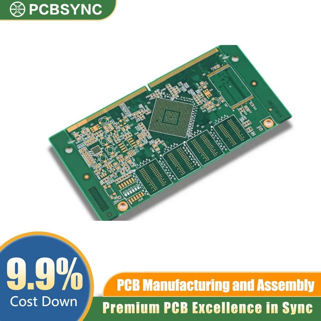
For hardware engineers developing compact, high-performance electronics, our custom sequential lamination HDI PCB stackup provides the necessary routing architecture for dense component placement. This custom build-up utilises repeated pressing and drilling cycles, enabling complex via structures that standard multilayer boards cannot accommodate.
Key Features of Sequential Lamination HDI PCBs
-
Via Technology: Supports blind, buried, staggered, and stacked microvias.
-
Custom Build-Up Options: Available in various structures including 1+N+1, 2+N+2, 3+N+3, and any-layer HDI.
-
Materials: Compatible with FR4, high-TG FR4, Rogers, and advanced halogen-free laminates for superior thermal performance.
-
Line Width/Spacing: Precision etching down to 2 mil / 2 mil (50µm) for dense trace routing.
-
Pad Technology: Reliable via-in-pad plating for BGA and fine-pitch components.
-
Compliance: Manufactured to strict IPC Class 2 and IPC Class 3 standards.
Applications
Sequential lamination stackups are essential for industries requiring miniaturisation without compromising electrical performance:
-
Telecommunications and 5G network equipment
-
Advanced medical diagnostics and wearable health monitors
-
Aerospace and aviation navigation systems
-
Automotive ADAS and autonomous driving controllers
-
High-end computing and mobile devices
Why Choose PCBSYNC
PCBSYNC is a professional PCB fabrication, PCBA, and EMS manufacturer delivering precision-built electronics for aerospace, medical, automotive, industrial, and smart energy applications. We handle everything from rapid prototyping to mass production — including rigid, flexible, and rigid-flex PCBs, full turnkey assembly, component sourcing, AOI and X-ray inspection, and OEM/ODM support. Reliable boards. Consistent quality. From prototype to production — PCBSYNC.
Submit your Gerber files and stackup requirements today to begin manufacturing your custom sequential lamination boards. Request a quote to speak with our engineering team.