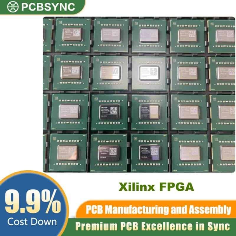
Xilinx XC7S50-1FTGB196Q Product Description
The AMD Xilinx XC7S50-1FTGB196Q is an advanced programmable logic device belonging to the cost-optimized Spartan-7 family. Built upon a 28nm High-Performance Low-Power (HPL) process technology utilizing high-k metal gate (HKMG) architecture, this Field Programmable Gate Array (FPGA) delivers an optimized balance between power conservation and high-speed processing capabilities. It is engineered specifically to meet the strict demands of automotive, industrial automation, consumer electronics, and communications systems where compact board dimensions and thermal control are priority constraints.
Technical Specifications and Hardware Architecture
The core architecture of the XC7S50-1FTGB196Q features 52,160 logic cells and 4,075 Configurable Logic Blocks (CLBs) powered by 6-input lookup table (LUT) technology. This flexible arrangement allows the chip to be configured as high-performance distributed memory or fast shift registers. The device includes 2,700 kbit of embedded block RAM (EBR) equipped with built-in FIFO control logic to streamline on-chip data buffering. Additionally, integrated Clock Management Tiles (CMTs), composed of Phase-Locked Loops (PLLs) and Mixed-Mode Clock Managers (MMCMs), ensure low-jitter, highly flexible system clock distribution.
Core Architecture and Hardware Matrix
For an accurate analysis of structural performance, the key hardware specifications are outlined in the data matrix below:
| Technical Parameter |
Specification Value |
| Manufacturer |
AMD Xilinx |
| Family Series |
Spartan®-7 |
| Part Number |
XC7S50-1FTGB196Q |
| Logic Cells / Elements |
52,160 |
| Number of LABs / CLBs |
4,075 |
| Total Block RAM Bits |
2,764,800 Bits (2.76 Mbit) |
| Distributed RAM Capacity |
600 kbit |
| Max Operating Frequency |
464 MHz |
Electrical, Package, and Environmental Standards
Operating requirements and physical attributes for implementation onto circuit boards include:
| Physical & Electrical Attribute |
Specification Value |
| Number of User I/Os |
100 I/O Pins |
| Core Supply Voltage Range |
0.95V ~ 1.05V (1.0V Nominal) |
| I/O Supply Voltage Range |
1.2V ~ 3.3V |
| Operating Temperature Range |
-40°C ~ +125°C (Junction Temperature $T_J$) |
| Package / Case Style |
196-LBGA, CSPBGA |
| Supplier Device Package Size |
196-CSBGA ($15 \times 15 \text{ mm}$) |
| Mounting Configuration |
Surface Mount (SMD / SMT) |
| Moisture Sensitivity Level |
MSL 3 (168 Hours Floor Life) |
Target Applications and System Integration
Thanks to its compact $15 \times 15 \text{ mm}$ CSBGA-196 package and an operating temperature rating up to 125°C, the automotive-qualified Q-grade XC7S50-1FTGB196Q variant is highly suitable for deployment in challenging environments. It is widely used in sensor fusion nodes, edge-based computer vision hardware, real-time motor drive control, and handheld instruments. The chip also features dual 12-bit analog-to-digital converters (XADC) with built-in thermal and power supply monitoring, adding robust diagnostic utility without requiring external components.
For engineering teams looking to seamlessly deploy high-density processing arrays onto custom hardware assemblies, choosing the right production partner is essential. Learn how specialized manufacturing services ensure strict physical tolerance compliance for complex BGA footprints by exploring high-reliability fabrication options for your next Xilinx FPGA design layout.
Deepen Your Knowledge
For visual learners seeking a hands-on guide to utilizing this specific silicon family in hardware designs, check out this Spartan 7 Schematic Design Tutorial. This video details the selection and electrical schematic design breakdown when configuring the XC7S50 system architecture.