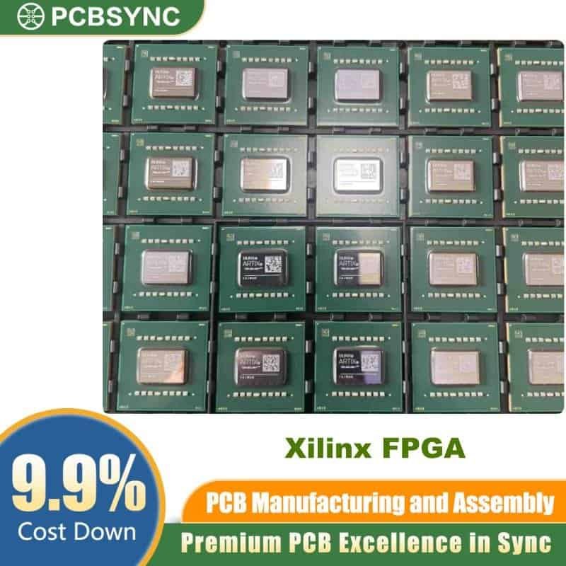
XC7S6-L1CSGA225I Product Description
The XC7S6-L1CSGA225I is a low-power, cost-optimized Field Programmable Gate Array (FPGA) belonging to the prominent AMD Xilinx FPGA Spartan-7 family. Built on an advanced 28nm High-K Metal Gate (HKMG) process technology, this specific “L1” low-power variant is designed to operate at reduced core voltages ($0.92\text{V}$ to $0.98\text{V}$), cutting static power consumption up to 50% compared to previous 45nm architectures. Packaged in a compact 225-ball Chip Scale Ball Grid Array (CSGA225), it provides an exceptionally high I/O pin-to-board-space ratio, making it an ideal choice for space-constrained embedded systems and dense printed circuit board assemblies (PCBA).
Core Architecture and Hardware Resources
At the center of the XC7S6-L1CSGA225I architecture are 6,000 logic cells organized across 469 Logic Array Blocks (LABs), utilizing flexible 6-input lookup tables (LUTs) that can double as distributed RAM. For data buffering, it integrates 180 kbits of block RAM alongside a total embedded RAM capacity of 184,320 bits. Hardware-accelerated math operations are handled by 10 dedicated DSP slices, allowing the chip to compute complex mathematical algorithms efficiently without overwhelming the core logic. Clock management is driven by a powerful Clock Management Tile (CMT) containing phase-locked loops (PLLs) and Mixed-Mode Clock Managers (MMCMs) to provide low-jitter, high-frequency synchronization up to $464\text{MHz}$.
Industrial Application and PCBA Integration
Engineered for industrial deployment, this IC features an operating temperature range of $-40^\circ\text{C}$ to $+100^\circ\text{C}$ ($T_J$). It breaks out 100 user I/Os through its 13x13mm CSGA225 package, supporting flexible I/O voltage standards from $1.2\text{V}$ up to $3.3\text{V}$. Designers frequently utilize this low-power semiconductor for industrial sensor fusion, legacy memory interface bridging, motor control logic, and networking control plane data transmission. It also integrates an internal dual 12-bit XADC system alongside on-chip thermal monitoring to actively report board-level health.
Technical Specifications: XC7S6-L1CSGA225I
The following data table outlines the complete parameters required for schematic design, circuit simulation, and SMT manufacturing deployment.
| Technical Parameter |
Specification Value |
| Manufacturer |
AMD / Xilinx |
| Product Series |
Spartan-7 (XC7S6) |
| Part Number Extension |
L1 (Low-Power Speed Grade) |
| Logic Elements / Cells |
6,000 |
| Number of LABs / CLBs |
469 |
| Total Block RAM Bits |
180 kbit (184,320 total bits) |
| Number of User I/Os |
100 I/O |
| Core Supply Voltage |
$0.92\text{V}$ to $0.98\text{V}$ ($0.95\text{V}$ Nominal) |
| Operating Temperature |
$-40^\circ\text{C}$ to $+100^\circ\text{C}$ (Industrial Grade) |
| Package / Case Style |
225-LFBGA, CSPBGA (13×13 mm) |
| Mounting Type |
Surface Mount Technology (SMT / SMD) |
| Moisture Sensitivity Level |
MSL 3 (168 Hours) |
Security and Development Workflow
The XC7S6-L1CSGA225I ensures data protection through hardware-level 256-bit AES encryption with HMAC/SHA-256 validation alongside automatic Single Event Upset (SEU) error detection and correction. Development is fully optimized under the Xilinx Vivado Design Suite, permitting engineers to implement MicroBlaze soft-core processors running above 200 DMIPs with comprehensive IP reuse, shortening the hardware engineering development loop.