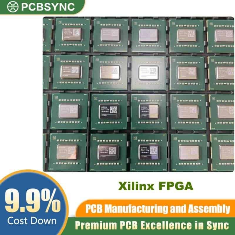
XC7S50-1CSGA324C Product Overview
The XC7S50-1CSGA324C is a highly efficient, low-power Field Programmable Gate Array (FPGA) belonging to the prominent Spartan-7 family from AMD Xilinx. Built on advanced 28nm high-k metal gate (HKMG) process technology, this integrated circuit is engineered to address the specific needs of cost-sensitive, high-volume applications without compromising on architectural throughput or logic capability.
Featuring 52,160 logic cells and 4,075 Configurable Logic Blocks (CLBs), the device delivers exceptional performance-per-watt metrics. The integration of 210 customizable user I/O pins within a compact 15x15mm Chip Scale BGA package (CSGA324) enables rich connectivity interfaces in hardware-constrained environments. For complex embedded processing, hardware designers can seamlessly deploy the MicroBlaze soft processor core inside this Xilinx FPGA architecture to achieve optimal system-level optimization.
Technical Specifications Table
The core electrical and hardware architecture metrics for the XC7S50-1CSGA324C are structured below for quick technical reference:
| Product Attribute |
Technical Specification Value |
| Manufacturer |
AMD / Xilinx |
| Part Number |
XC7S50-1CSGA324C |
| Product Series |
Spartan-7 XC7S50 |
| Number of Logic Cells |
52,160 Logic Cells |
| Configurable Logic Blocks (CLBs) |
4,075 LABs / 8,150 Slices |
| Total Embedded Block RAM (BRAM) |
2,700 Kbit (Maximum 337.5 kB) |
| Maximum Distributed RAM |
600 Kbit |
| DSP Slices |
120 Slices |
| Number of User I/Os |
210 User I/O Pins |
| Core Supply Voltage Range |
0.95 V to 1.05 V (1.0 V Nominal) |
| I/O Supply Voltage Range |
1.2 V to 3.3 V |
| Operating Temperature Range |
0°C to 85°C (Junction Temperature) |
| Package / Case Material |
324-LFBGA, CSPBGA (15×15 mm Size) |
| Speed Grade |
-1 Speed Grade |
Key Features and Architectural Benefits
High-Efficiency Power Management
Operating within a strict core voltage window of 0.95V to 1.05V, the Spartan-7 chip architecture minimizes static power dissipation. The 28nm HPL processing node significantly lowers system thermals, enabling reliable thermal dissipation inside small, enclosed multi-layer PCB assemblies.
Memory Layout and Internal DSP Capacity
The platform contains 2,700 Kbits of dual-port block RAM alongside a maximum configuration of 600 Kbits of distributed RAM. This versatile memory hierarchy is augmented by 120 dedicated DSP slices, allowing hardware designs to perform real-time digital filtering, complex arithmetic calculations, and fast signal manipulation.
Clock Management and Analog Integration
System timing synchronization is stabilized via 5 Clock Management Tiles (CMTs), combining specialized Phase-Locked Loops (PLLs) and Mixed-Mode Clock Managers (MMCMs). Additionally, the device embeds an internal 12-bit dual-channel XADC block capable of handling 1 MSPS analog-to-digital conversions alongside internal thermal monitoring telemetry.
Primary Industrial Applications
Industrial Automation and Motor Control
The high User I/O concentration (210 pins) coupled with precision analog XADC blocks makes this IC ideal for real-time motor controller units, high-density sensor processing nodes, and multi-axis industrial robotic control boards.
Machine Vision Capture Systems
The chip functions seamlessly as a low-latency data format bridge, establishing reliable connectivity paths between modern image arrays and central application host processors while executing custom pixel-level filtering.
Secure Internet of Things (IoT) Edge Nodes
Built-in security frameworks, including 256-bit AES encryption support and HMAC/SHA-256 authenticators, provide robust cryptographic safeguards for edge data aggregators.