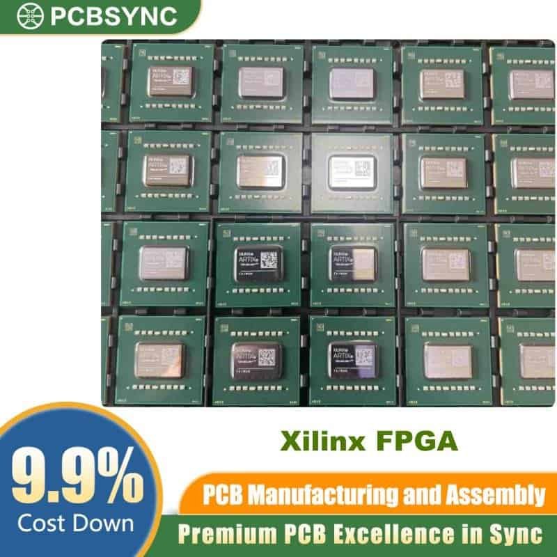
The Xilinx XC7VX1140T-1FLG1928I is a high-end Virtex-7 XT field-programmable gate array engineered for designers who need maximum logic density, DSP throughput, and serial bandwidth inside a single device. Built on TSMC’s 28 nm high-k metal gate (HKMG) HPL process and assembled using Stacked Silicon Interconnect (SSI) technology, the chip integrates 1,139,200 logic cells into a rugged 1928-pin FCBGA package. Furthermore, it runs on a 1.0 V core supply and is industrial-grade screened for −40 °C to 100 °C junction temperatures, making it ideal for 24/7 operation.
Why Choose the XC7VX1140T-1FLG1928I?
This device is the largest member of the Virtex-7 XT line. As a result, it delivers up to 1.4 Tb/s of I/O bandwidth, 4.7 TMAC/s of DSP performance, and roughly 50% lower power than the previous Virtex-6 generation. Moreover, its 96 GTH multi-gigabit transceivers support line rates up to 13.1 Gb/s—an excellent fit for 100G/400G networking, OTN line cards, software-defined radio, ASIC prototyping, advanced medical imaging, and aerospace systems.
Key Technical Specifications
| Parameter |
Value |
| Manufacturer |
AMD / Xilinx |
| Family |
Virtex-7 XT |
| Logic Cells |
1,139,200 |
| CLB Slices |
178,000 |
| CLB Flip-Flops |
1,424,000 |
| Max Distributed RAM |
17,700 Kb |
| Block RAM (36 Kb) |
1,880 blocks / 67,680 Kb |
| DSP48E1 Slices |
3,360 |
| Process Node |
28 nm HKMG HPL |
| Core Voltage (VCCINT) |
0.97 V – 1.03 V |
| Speed Grade |
−1 (standard) |
| Temperature Grade |
Industrial (−40 °C to 100 °C) |
Connectivity, I/O & Package Details
| Feature |
Specification |
| GTH Transceivers |
96 channels, up to 13.1 Gb/s |
| User I/O (HP) |
480 |
| PCI Express Hard Blocks |
4 × Gen2 ×8 |
| Clock Management Tiles |
24 (each with MMCM + PLL) |
| XADC |
Dual 12-bit, 1 MSPS ADC |
| Memory Interface |
DDR3 up to 1,866 Mb/s |
| Package |
FLG1928 — 1928-ball Pb-free FCBGA |
| Body Size |
45 × 45 mm |
Applications and Design Tool Support
Engineers typically deploy this Xilinx FPGA in wired-communication backplanes, defense radar, high-frequency trading accelerators, and broadcast video processing—anywhere capacity and transceiver count cannot be compromised. In addition, designs are developed in Vivado Design Suite, with full support for IP cores, partial reconfiguration, and SystemVerilog/VHDL flows. Reference designs and pinout files are also available from AMD Xilinx documentation.
Order the XC7VX1140T-1FLG1928I with Confidence
Every XC7VX1140T-1FLG1928I we supply is sourced through authorized channels, shipped in original anti-static packaging, and backed by a full quality guarantee. Request a quote today for competitive pricing, fast lead times, and worldwide shipping.