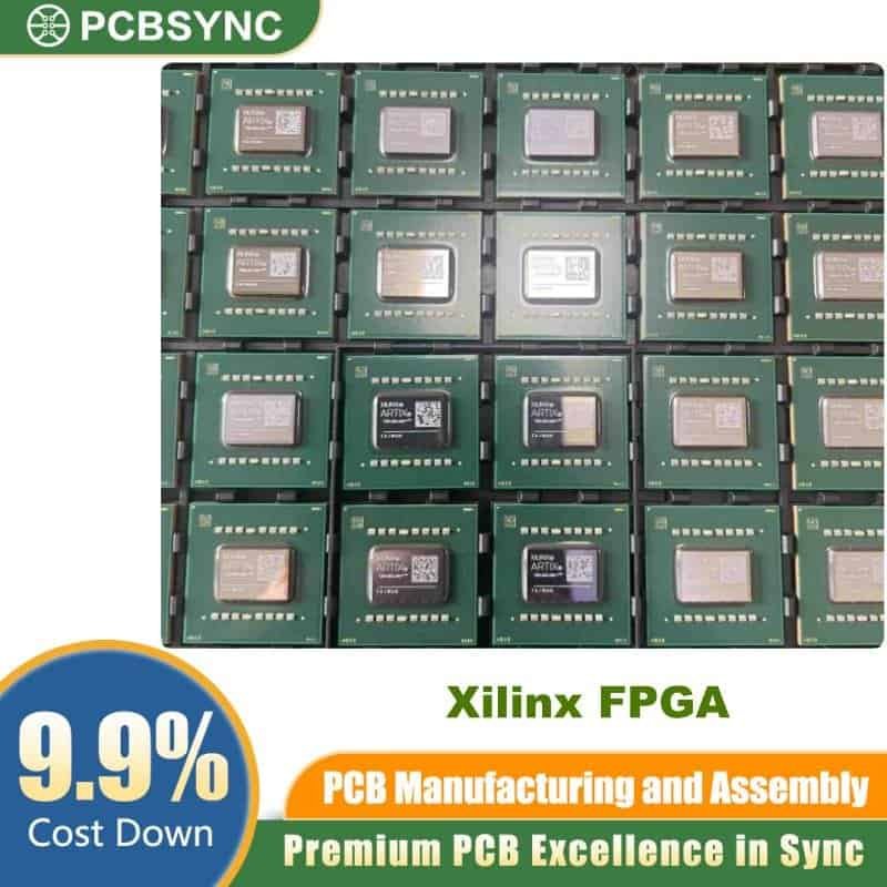
The XC7VX485T-1FFG1761C is a high-performance Field Programmable Gate Array from AMD’s Virtex-7 XT family, built on TSMC’s 28 nm HKMG (High-K Metal Gate) process. With 485,760 logic cells, 56 GTX multi-gigabit transceivers, and 700 user I/Os packed into a 1761-ball flip-chip BGA, the XC7VX485T-1FFG1761C is engineered for bandwidth-intensive designs in wired communications, radar, ASIC prototyping, and data-center acceleration.
Why Choose the XC7VX485T-1FFG1761C?
Virtex-7 XT devices are optimized for transceiver-heavy workloads, and the XC7VX485T-1FFG1761C delivers that balance of logic density, DSP throughput, and serial I/O that most -485T designs need. The “-1” speed grade and commercial temperature rating (0 °C to 85 °C) make it a cost-effective pick for lab, industrial, and production hardware where you still want the full pin-out of the 1761 package for maximum I/O and transceiver access.
Sourcing tip: for authorized stock, cross-reference, and PCB assembly support for this part, browse the full Xilinx FPGA catalog.
XC7VX485T-1FFG1761C Part Number Breakdown
| Code Segment |
Meaning |
| XC |
Commercial product prefix |
| 7V |
7 Series Virtex family |
| X485T |
Virtex-7 XT, ~485K logic cells |
| -1 |
Speed grade 1 (standard) |
| FFG1761 |
Flip-chip fine-pitch BGA, 1761 balls, Pb-free |
| C |
Commercial temp range (0 °C to 85 °C) |
Key Technical Specifications
Logic, Memory & DSP Resources
| Parameter |
Value |
| Logic Cells |
485,760 |
| CLB Slices |
75,900 |
| CLB Flip-Flops |
607,200 |
| DSP48E1 Slices |
2,800 |
| Peak DSP Performance |
2,800 GMAC/s |
| Block RAM (36 Kb blocks) |
1,030 |
| Total Block RAM |
37,080 Kb |
| CMTs (MMCM + PLL) |
14 |
High-Speed Serial & I/O
| Parameter |
Value |
| GTX Transceivers |
56 (up to 10.3125 Gb/s) |
| Integrated PCIe Blocks |
4 × PCIe Gen2 x8 |
| Maximum User I/O |
700 |
| I/O Standards |
HP 1.2 V–1.8 V, HR 1.2 V–3.3 V |
| Memory Interface Support |
DDR3 up to 1,866 Mb/s |
| XADC |
Dual 12-bit 1 MSPS ADC |
Package, Process & Environment
| Parameter |
Value |
| Process Technology |
28 nm HKMG HPL |
| Package |
FCBGA-1761 (flip-chip, Pb-free) |
| Body Size |
42.5 × 42.5 mm, 1.0 mm pitch |
| Core Voltage (VCCINT) |
1.0 V |
| Operating Temperature |
0 °C to +85 °C (Commercial) |
| Security |
256-bit AES + HMAC/SHA-256, SEU detect & correct |
Typical Applications of the XC7VX485T-1FFG1761C
Wired & Wireless Communications
Line cards, OTN framers, and 10G–40G packet processing that benefit from 56 GTX lanes and integrated PCIe Gen2 x8 host interfaces.
ASIC Prototyping & Emulation
The 485K-logic-cell capacity and 1761-pin break-out make the XC7VX485T-1FFG1761C a mainstay on emulation boards such as the VC707 reference platform.
Radar, SDR & Signal Processing
2,800 DSP48E1 slices with 25×18 multipliers and pre-adders accelerate FIR filters, FFTs, and beamforming pipelines.
Video, Imaging & Data Center Acceleration
High block-RAM count and wide I/O support real-time video processing, 4K transcoding, and PCIe-attached compute offload cards.
Design Tool Support
The XC7VX485T-1FFG1761C is fully supported by AMD Vivado Design Suite, with mature IP for PCIe, Ethernet, DDR3/DDR4, AXI, and Aurora. Legacy ISE flows are not supported on Virtex-7 XT.