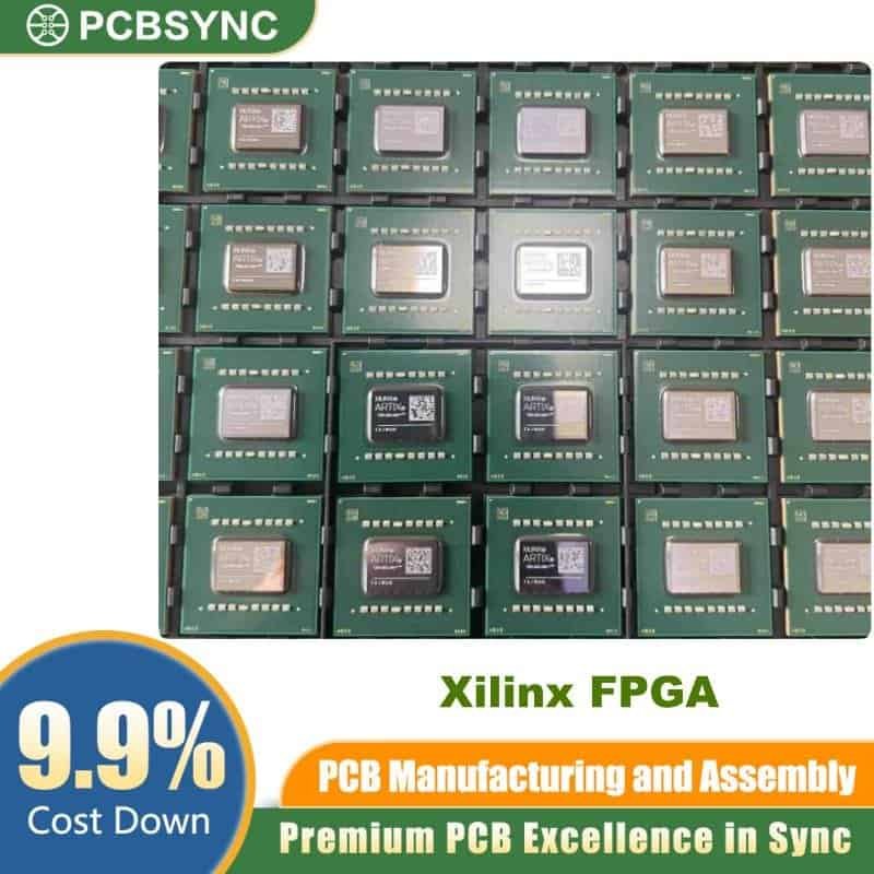
The XC7VX485T-2FF1761I is a high-performance Field Programmable Gate Array from the AMD Virtex-7 XT family, engineered for bandwidth-intensive and compute-heavy applications. Built on state-of-the-art, high-performance, low-power (HPL), 28 nm, high-k metal gate (HKMG) process technology FPGAkey, this industrial-grade device delivers exceptional logic density, DSP throughput, and serial I/O bandwidth in a rugged 1761-ball flip-chip BGA package. Engineers choose this Xilinx FPGA for 10G–100G networking, radar signal processing, ASIC prototyping, and PCIe-based data-center accelerators.
Key Features and Benefits
The XC7VX485T-2FF1761I offers an unmatched balance of performance-per-watt and system integration. With 1.4 Tb/s of I/O bandwidth, 980K logic cell capacity, and 4.7 TMAC/s DSP FPGAkey at the family level, it provides a fully programmable alternative to ASSPs and ASICs. Its advanced 6-input LUT fabric, hardened PCIe block, and GTX/GTH transceivers make it ideal for designs requiring deterministic latency and massive parallelism.
Core Highlights
- 485,760 logic cells for complex control and data-path logic
- 700 user I/Os supporting HP and HR standards
- 37,080 Kbit of 36KB dual-port Block RAM with built-in FIFO logic
- 2,800 DSP48E1 slices with 25×18 multiplier and 48-bit accumulator
- GTX transceivers up to 12.5 Gb/s for high-speed serial links
- Integrated PCIe block (x8 Gen2 on this device)
- 256-bit AES encryption with HMAC/SHA-256 authentication and SEU correction
XC7VX485T-2FF1761I Technical Specifications
General Electrical & Logic Parameters
| Parameter |
Value |
| Manufacturer |
AMD (Xilinx) |
| Device Family |
Virtex-7 XT |
| Process Technology |
28 nm HKMG |
| Logic Cells |
485,760 |
| CLBs (Slices) |
75,900 |
| Block RAM |
37,080 Kbit (1,030 × 36Kb) |
| DSP48E1 Slices |
2,800 |
| Max Operating Frequency |
710 MHz |
| Core Voltage (VCCINT) |
0.97 V – 1.03 V |
| I/O Voltage (VCCO) |
Up to 3.3 V |
Package, I/O & Environmental Data
| Parameter |
Value |
| Package |
FCBGA (Flip-Chip BGA) |
| Pin Count |
1761 balls |
| Package Size |
42.5 × 42.5 mm |
| User I/Os |
700 |
| I/O Banks |
HP + HR |
| Speed Grade |
–2 |
| Temperature Grade |
Industrial (–40 °C to +100 °C TJ) |
| PCIe Support |
x8 Gen2 (hardened block) |
| Transceivers |
GTX up to 12.5 Gb/s |
| RoHS |
Compliant |
Typical Applications
The XC7VX485T-2FF1761I is deployed in wired and wireless communications infrastructure, software-defined radio, medical imaging, aerospace and defense systems, high-frequency trading cards, and FPGA-based accelerator boards. Its industrial temperature rating and hardened security features also make it well-suited for deployed edge systems where reliability is critical.
Design Tools and Support
This device is fully supported by AMD’s Vivado Design Suite, which provides synthesis, implementation, timing closure, and debug flows optimized for the 7 Series architecture. Legacy ISE flows are also supported, but Vivado is recommended for new designs.