Engineered for Precision. Built for Performance.
The PCBSYNC 12-Layer 50μ” Hard Gold Plating PCB represents the pinnacle of advanced printed circuit board manufacturing, delivering uncompromising electrical performance, mechanical durability, and surface finish quality for the most demanding industrial, aerospace, defense, and high-frequency telecommunications applications.
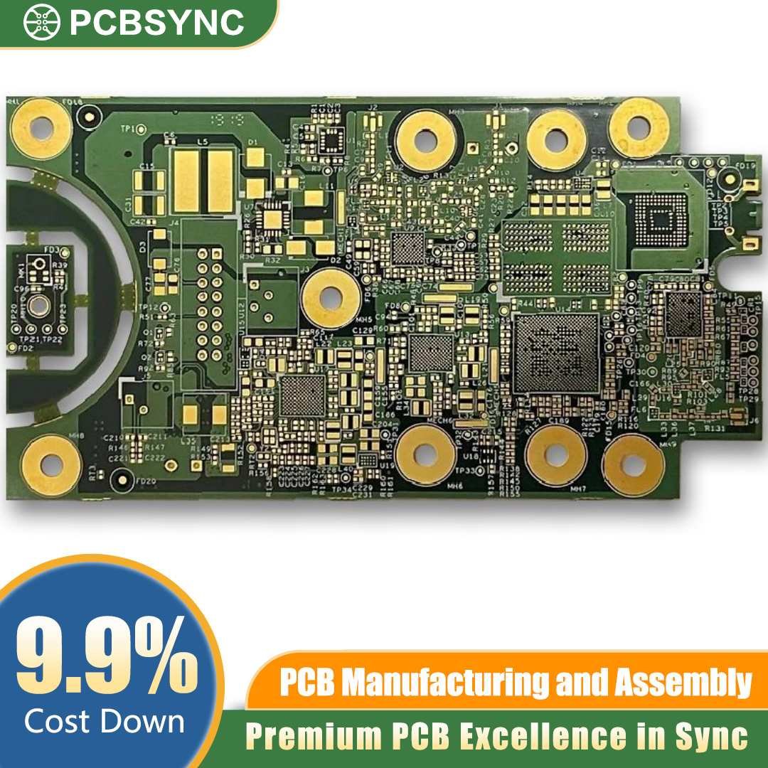
Exceptional Multilayer Architecture
At its core, this PCB features a 12-layer stackup meticulously engineered to support complex signal routing, superior impedance control, and outstanding electromagnetic interference (EMI) shielding. The multilayer construction enables dense component integration without sacrificing signal integrity, making it the ideal solution for high-density interconnect (HDI) designs, RF/microwave circuits, and mission-critical embedded systems.
Each layer is precisely laminated using high-quality FR4 or high-Tg base materials, ensuring dimensional stability across wide temperature ranges and resistance to delamination under thermal cycling stress. The controlled dielectric constant across all layers guarantees consistent impedance values — critical for high-speed digital and analog signal transmission.
Industry-Leading 50μ” Hard Gold Surface Finish
What truly sets this PCB apart is its 50 microinch (50μ”) Hard Gold Electroplating finish — a premium surface treatment far exceeding the standard 30μ” specification commonly found in commercial-grade boards.
Hard gold plating, composed of gold-cobalt alloy, is deposited through a precise electroplating process, producing a surface with:
-
Exceptional wear resistance — withstanding 10,000+ mating cycles without degradation
-
Outstanding contact reliability — ensuring consistent, low-resistance electrical connections
-
Superior corrosion and oxidation resistance — maintaining surface integrity in harsh environments
-
Excellent solderability — supporting reliable solder joint formation during assembly
The 50μ” thickness specification makes this finish particularly suitable for edge connectors, gold fingers, sliding contacts, keypads, test points, and any application where mechanical abrasion and repeated contact are unavoidable.
Key Technical Specifications
| Parameter |
Specification |
| Layer Count |
12 Layers |
| Surface Finish |
Hard Gold Plating (Au-Co Alloy) |
| Gold Thickness |
50μ” (1.27μm) |
| Nickel Underlay |
100–200μ” |
| Base Material |
FR4 / High-Tg FR4 |
| Min. Trace/Space |
3/3 mil |
| Board Thickness |
1.6mm (custom available) |
| Max. Aspect Ratio |
10:1 |
| Copper Weight |
1oz – 2oz (inner/outer) |
| Surface Flatness |
≤0.75% bow and twist |
Applications
PCBSYNC’s 12-Layer Hard Gold PCB serves across multiple high-performance sectors:
-
Aerospace & Defense — avionics control modules, radar systems
-
Medical Devices — diagnostic equipment, implantable electronics
-
Telecommunications — 5G infrastructure, high-frequency switching
-
Industrial Automation — servo controllers, robotic systems
-
Consumer High-End Electronics — gaming hardware, GPU interconnects
Why Choose PCBSYNC?
PCBSYNC combines ISO 9001-certified manufacturing processes, rigorous IPC-A-600 Class 3 inspection standards, and advanced AOI/X-ray testing to deliver boards with zero-defect assurance. Every 12-layer hard gold PCB undergoes 100% electrical testing, impedance verification, and final cosmetic inspection before shipment.
PCBSYNC — Where precision meets reliability, every layer, every trace, every connection.


 Motor Stator")


