Inquire: Call 0086-755-23203480, or reach out via the form below/your sales contact to discuss our design, manufacturing, and assembly capabilities.
Quote: Email your PCB files to Sales@pcbsync.com (Preferred for large files) or submit online. We will contact you promptly. Please ensure your email is correct.
Notes: For PCB fabrication, we require PCB design file in Gerber RS-274X format (most preferred), *.PCB/DDB (Protel, inform your program version) format or *.BRD (Eagle) format. For PCB assembly, we require PCB design file in above mentioned format, drilling file and BOM. Click to download BOM template To avoid file missing, please include all files into one folder and compress it into .zip or .rar format.
Every time you open a schematic, you’re reading a language. And in that language, the capacitor symbol is one of the most frequently used words — appearing dozens of times in a typical power supply design, hundreds of times in a complex digital board. Get the symbol right and you communicate clearly: the right component, the right polarity, the right function. Get it wrong and you risk reversed electrolytics, misidentified bypass caps, or assembly errors that don’t show up until a prototype comes back from the fab.
This guide covers every capacitor symbol you’ll encounter across IEC, ANSI/IEEE, and JIS standards — what each one looks like, what it means, where it comes from, and how to use it correctly in your schematics. Aimed at working PCB engineers and serious hobbyists who need to read and draw schematics accurately, not just recognize a pair of parallel lines.
## What a Capacitor Symbol Actually Represents
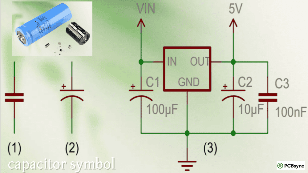
The basic capacitor symbol is a direct visual abstraction of the physical structure it represents: two conductive plates separated by a gap (the dielectric). The connecting wires represent the leads. That’s it. The simplicity is the point — the symbol communicates the core functional idea (charge can accumulate between these plates) without getting into dielectric material, package type, or ESR characteristics. Those details belong in the component fields and the BOM, not in the symbol artwork.
This separation of concerns is important to understand: the capacitor symbol on a schematic tells you the electrical function and polarity. It does not tell you the package (0402 vs through-hole radial), the dielectric class (C0G, X7R, electrolytic), the voltage rating, or the ESR. All of those live in the component attributes attached to the symbol — the fields you see when you click on a part in KiCad, Altium, or any other EDA tool.
Two standards bodies govern how capacitor symbols are drawn in professional schematics, and they make visually different choices for several symbol types. Running into a schematic from a European supplier when you’re used to American datasheets — or vice versa — is a common source of confusion. Knowing both systems eliminates it.
### ANSI/IEEE 315 (North American Standard)
ANSI/IEEE 315, also known as IEEE Std 315, is the American standard for graphic symbols in electrical and electronics diagrams. It was developed by IEEE and adopted by ANSI. Under this standard, schematics from US companies like Texas Instruments, Microchip, and Analog Devices are drawn. Key characteristics of the ANSI/IEEE capacitor symbol approach:
The non-polarized capacitor is drawn as two parallel straight lines of equal length, separated by a gap, with leads extending from each line perpendicularly. Both plates look identical, clearly indicating no polarity preference.
The polarized capacitor uses one straight plate and one curved plate. The curved plate is universally the negative (−) terminal, the cathode. The straight plate is positive (+). A “+” sign is often added explicitly next to the straight plate as confirmation. This curved-negative convention is the most important thing to commit to memory for ANSI/IEEE schematics.
### IEC 60617 (International Standard)
IEC 60617 is the International Electrotechnical Commission’s standard for graphical symbols, dominant in European and internationally-oriented schematics from companies like Siemens, Philips, and STMicroelectronics. Under IEC 60617:
The non-polarized capacitor is drawn using two parallel rectangles (sometimes described as short filled bars) rather than simple lines, giving it a slightly heavier, boxier appearance. Functionally identical to the ANSI version but visually distinct.
The polarized capacitor in IEC 60617 uses a straight plate for the positive terminal and a curved plate for negative — the same plate convention as ANSI/IEEE. The key difference is that IEC schematics rely more heavily on the explicit “+” sign annotation near the positive terminal rather than relying on plate shape alone to convey polarity.
### JIS (Japanese Industrial Standard)
JIS C 0617 was derived from IEC 60617, so modern Japanese schematics generally follow IEC symbol forms for capacitors, with minor variations. Older Japanese schematics from periods of strong US technical influence may use ANSI-style symbols. If you’re working with Japanese electronics documentation, check which era the schematic is from to determine which style to expect.
ANSI/IEEE vs IEC Capacitor Symbol Comparison:
Feature
ANSI/IEEE 315
IEC 60617
Non-polarized symbol
Two thin parallel lines
Two parallel rectangles/bars
Polarized symbol
Straight plate (+) + curved plate (−)
Straight plate (+) + curved plate (−), with explicit “+”
Polarity indication
Curved plate = negative; “+” near straight plate
“+” marking; curved = negative
Dominant regions
USA, Canada
Europe, Asia, international projects
Typical EDA defaults
Altium (US-style), Eagle (mixed)
KiCad (IEC-leaning), Cadence (both)
Standard document
IEEE Std 315 / ANSI Y32.2
IEC 60617-4
One important rule for schematic quality: never mix IEC and ANSI symbol styles within a single schematic. A “Franken-schematic” that combines both creates ambiguity for reviewers, assembly engineers, and automated tools that parse schematic data. Choose one standard and apply it consistently across the entire design.
## Complete Capacitor Symbol Reference by Type
### Non-Polarized Capacitor Symbol
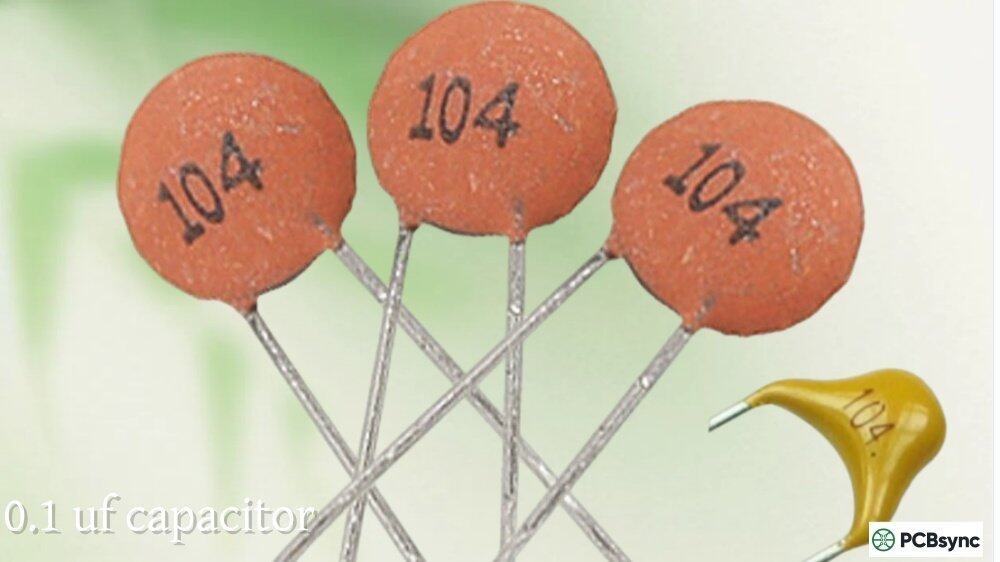
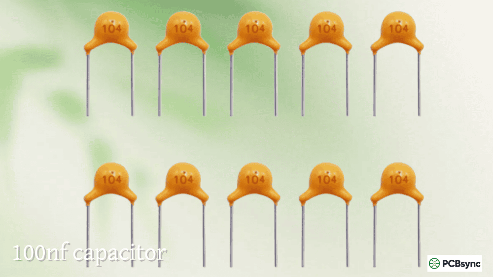
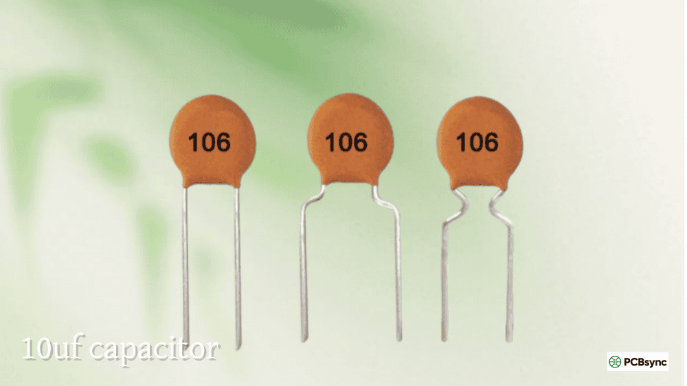
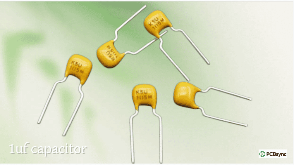
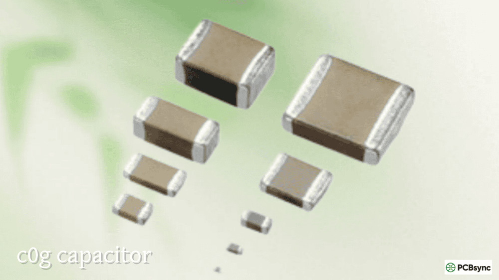
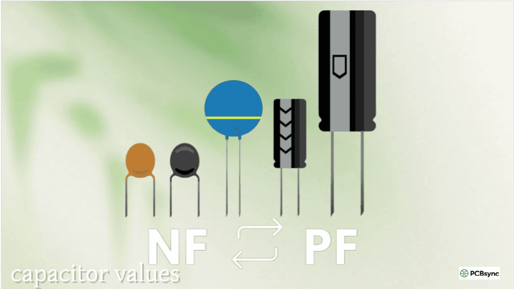
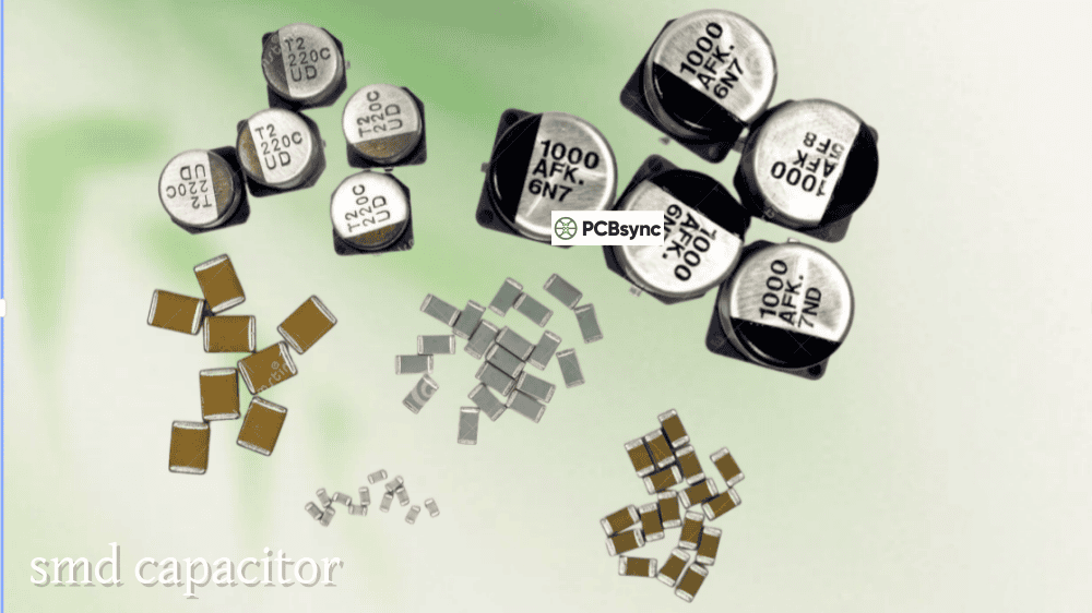
The non-polarized capacitor symbol is the most fundamental form. Two identical parallel plates, a gap between them, leads coming off each plate. No marking, no curved line, no polarity indicator of any kind. This is correct and intentional: non-polarized capacitors (ceramic disc, MLCC, mica, film, polypropylene) can be connected either way in a circuit without consequence or damage.
In context on a schematic, you’ll see this symbol used for bypass and decoupling caps on IC power pins (typically 100nF ceramic), signal coupling capacitors between amplifier stages, filter capacitors in RC networks, and crystal load capacitors.
Reference designator: C (e.g., C1, C23, C104)
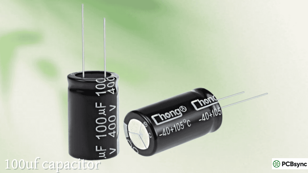
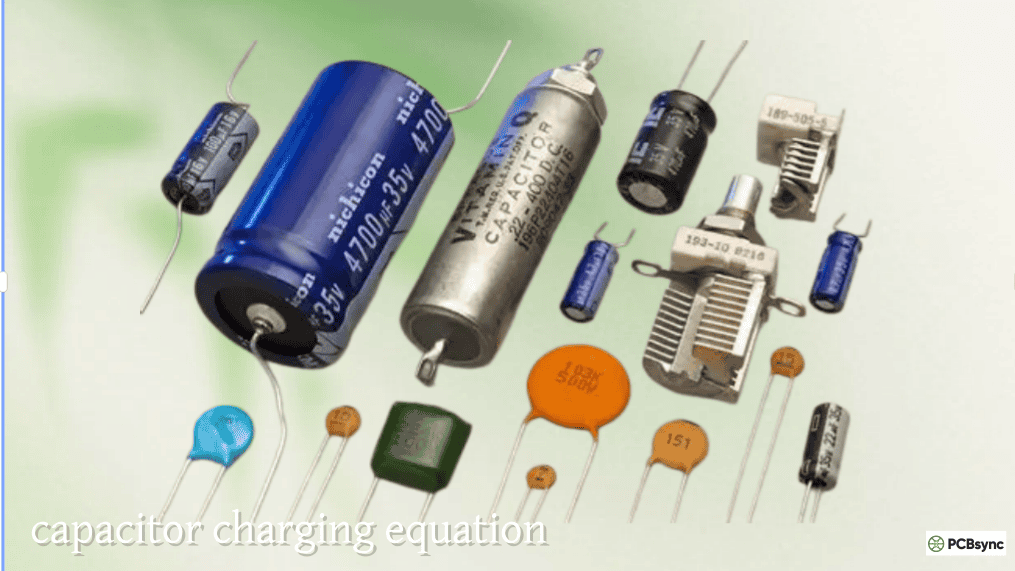
### Polarized Capacitor Symbol (Electrolytic and Tantalum)
The polarized capacitor symbol has two asymmetric plates: one straight, one curved. The curved plate represents the negative terminal (cathode) in both ANSI and IEC conventions, despite the two standards expressing polarity annotation differently. The “+” sign near the straight plate — or sometimes explicitly written as a separate text annotation — confirms the positive terminal.
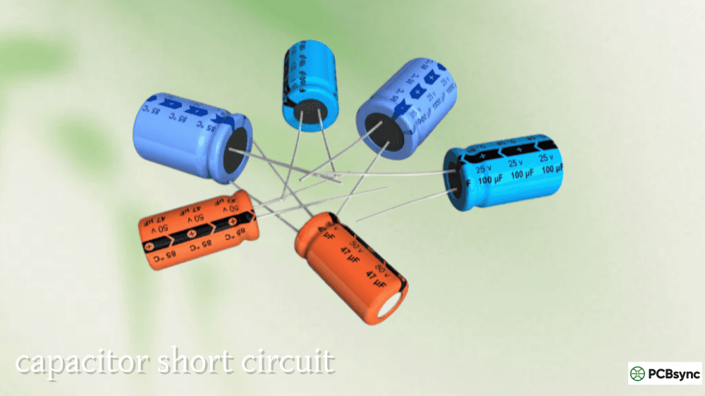
This symbol is used for aluminium electrolytic capacitors, tantalum capacitors, and niobium oxide capacitors: components with a defined polarity that will be damaged or destroyed if connected backwards. The failure mode is not subtle — reversed electrolytics generate hydrogen gas internally, which can rupture the vented top or, in a worst case, launch the component off the board entirely.
Reference designator: C (same prefix as non-polarized; polarity is carried in the symbol, not the designator)
Critical assembly note: The polarity marking on the physical component body does not always match intuitive expectations. On through-hole aluminium electrolytics, the stripe or minus-sign band on the sleeve marks the negative lead — and the shorter lead is also negative. On SMD tantalum capacitors, the polarity bar or stripe marks the positive (anode) terminal — the exact opposite of the electrolytic convention. This distinction causes real assembly errors when engineers are used to one type but working with the other.
### Variable Capacitor Symbol
The variable capacitor symbol takes the basic two-plate non-polarized symbol and adds a diagonal arrow passing through it. The arrow indicates that the capacitance value is user-adjustable — typically via a rotating shaft or knob that changes the degree of plate overlap. Variable capacitors appear in RF tuning circuits, old-school AM radio tuners, and antenna matching networks.
Reference designator: CV or VC (varies by convention)
### Trimmer Capacitor Symbol
The trimmer capacitor symbol is similar to the variable capacitor but uses a T-shaped or bent arrow overlay, or sometimes an annotation of “Tr” to distinguish it from a panel-accessible variable cap. Trimmers are factory-set or field-calibrated with a screwdriver and then left fixed. They appear in RF filter calibration, oscillator frequency fine-tuning, and impedance matching on antenna boards.
Reference designator: CV, CT, or trimmer-specific designator depending on the team’s convention
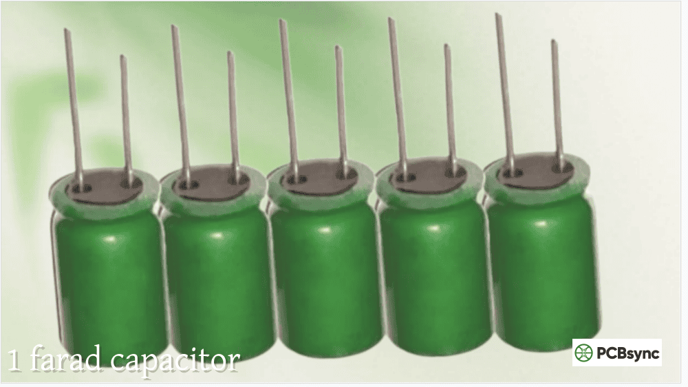
### Supercapacitor / Ultracapacitor Symbol
The supercapacitor symbol resembles a polarized electrolytic symbol (since most supercaps are polarized) but typically adds a box or rectangle drawn over one of the plates, or sometimes the label “UC” or “SC” is added near the symbol to distinguish it from a standard electrolytic. The distinction matters because a supercapacitor’s capacitance is measured in farads rather than microfarads — using a standard electrolytic symbol for a 10F part without any distinguishing marker would be confusing to anyone reading the schematic.
Reference designator: C (with value clearly stated in farads, e.g., “C45 10F 5.5V”)
### Ganged / Dual Variable Capacitor Symbol
Some RF designs use ganged capacitors — mechanically linked variable capacitors that adjust simultaneously. The schematic symbol shows two variable capacitor symbols connected by a dashed mechanical coupling line. This makes it immediately clear that these are not two independent adjustable capacitors but a single physical assembly that tunes both sections together.
All Capacitor Symbol Types — Quick Reference Table:
Symbol Type
Key Visual Feature
Typical Application
Standard Where Used
Non-polarized (ANSI)
Two equal parallel lines
Ceramic bypass, film coupling, mica RF
ANSI/IEEE 315
Non-polarized (IEC)
Two equal parallel rectangles
Same as above
IEC 60617
Polarized (ANSI)
Straight (+) plate + curved (−) plate
Electrolytic bulk, tantalum decoupling
ANSI/IEEE 315
Polarized (IEC)
Straight (+) plate + curved plate + explicit “+”
Same as above
IEC 60617
Variable capacitor
Non-polarized symbol + diagonal arrow through
RF tuning, antenna matching
Both
Trimmer capacitor
Non-polarized symbol + T-arrow or “Tr” annotation
Oscillator calibration, IF filter tuning
Both
Supercapacitor
Polarized symbol + box/UC annotation
Energy storage, backup power, EV systems
Both (no single standard)
Ganged capacitor
Two variable symbols + dashed mechanical link
AM radio, dual-section RF tuning
Both
Safety cap (X/Y)
Standard non-polarized + X1/X2/Y1/Y2 annotation
Mains EMI filtering
Both
## Understanding Polarity Symbols in Depth
Polarity errors are the most dangerous misread in schematic interpretation. The consequences range from a failed component on first power-up to a safety incident in mains-connected equipment. Getting polarity right requires understanding both the schematic symbol convention and the physical component marking — and knowing where they diverge.
### Reading Polarity in ANSI/IEEE Schematics
In ANSI/IEEE schematics, the rule is simple and consistent: the curved plate is always negative. Draw the “+” explicitly next to the straight plate as a redundancy check. When in doubt, look for the “+” — if it’s present near one terminal, that terminal is positive regardless of which plate shape is used (some schematic editors draw both plates straight and rely on the “+” exclusively).
### Reading Polarity in IEC Schematics
IEC 60617 uses the same plate-shape convention (straight = positive, curved = negative) but places more emphasis on the “+” annotation. In older IEC drawings and some European equipment schematics, you may also encounter a filled rectangle versus empty rectangle convention for positive and negative plates, though this is less common in modern EDA tools.
### Physical Marking vs Schematic Convention: The Tantalum Trap
The physical polarity marking on a component body is separate from the schematic symbol, and the two can seem contradictory if you’re not careful. Here is the critical comparison:
Physical Polarity Markings — Component Body:
Component Type
Physical Marking Convention
Positive Terminal
Through-hole aluminium electrolytic
Stripe / minus sign on sleeve
Longer lead; side without stripe
SMD aluminium electrolytic (V-chip)
Stripe on body
Side without stripe is positive
Through-hole tantalum
“+” printed on body
Side with “+” marking
SMD tantalum
Bar / stripe on body
Side with the stripe (opposite of electrolytic!)
Through-hole tantalum (older types)
Coloured band
Consult datasheet — convention varies
The SMD tantalum polarity reversal (stripe = positive, not negative) is the most frequent source of polarity assembly errors. An engineer familiar only with electrolytic conventions will reverse every SMD tantalum they hand-solder. Add silkscreen “+” and “−” markings on your PCB layout near all polarized SMD capacitor pads, and call out polarity explicitly in assembly drawings. This small effort eliminates a failure mode that can kill an entire batch of boards.
## Reference Designators and Schematic Annotation
### The “C” Designator
All capacitor symbols in a schematic carry the reference designator prefix “C”, followed by a sequential number: C1, C2, C3… up to however many capacitors are in the design. There is no distinction in the designator itself between a polarized and non-polarized capacitor — C47 could be a 100nF ceramic or a 1000µF electrolytic. The symbol shape carries the polarity information; the designator provides only a unique identifier.
In large designs, some teams use sub-block numbering (C100-series for the power supply block, C200-series for the RF section, etc.) to make the BOM and assembly notes easier to navigate. This is a team convention, not a standards requirement.
### What to Annotate Next to the Symbol
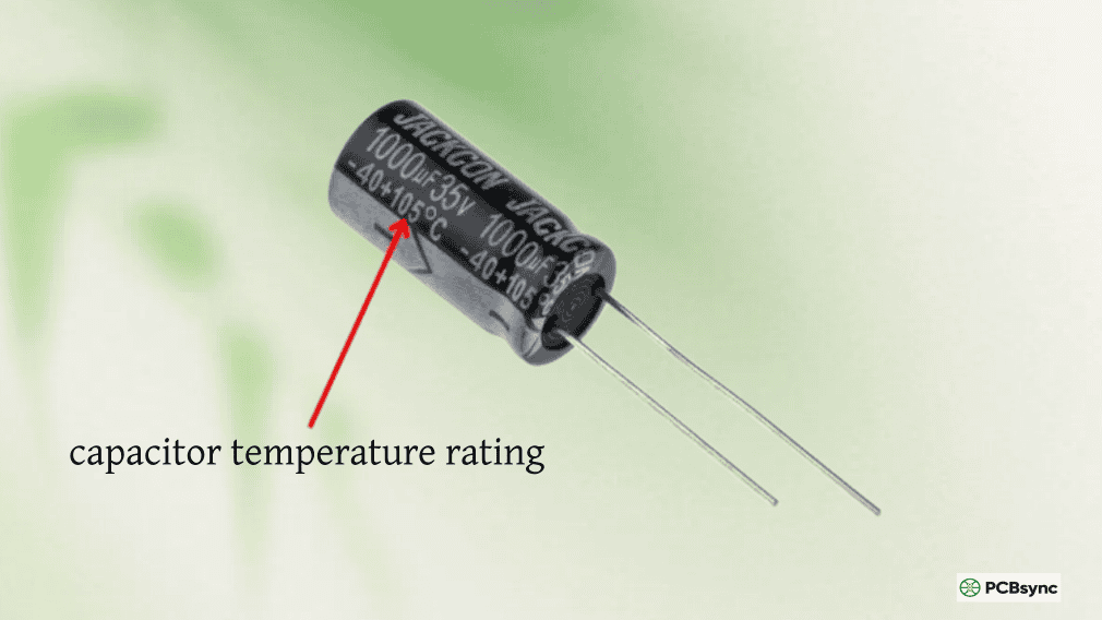
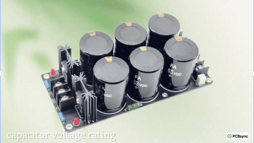
Capacitor symbols in a professional schematic carry at minimum: the reference designator, the capacitance value with units, and the voltage rating. For polarized caps, the voltage is non-negotiable — leaving it out means the assembler or reviewer has to look it up in the BOM, which costs time and introduces the risk of errors. For precision applications, tolerance and dielectric class (C0G, X7R) should also appear in the schematic annotation or component attribute block.
Capacitor Schematic Annotation — Minimum vs Best Practice:
Information Field
Minimum for Non-Critical Design
Best Practice
Reference designator
C1
C1
Capacitance value
100nF
100nF
Voltage rating
Optional for low-voltage signal caps
Always — e.g., 50V
Tolerance
Omit for bypass/decoupling
±10% or dielectric code
Dielectric class
Omit unless precision
C0G, X7R, X5R
Part number
Omit for generic placement
Include for fixed-source parts
## Capacitor Symbols in EDA Tools: Altium, KiCad, and Eagle
### How EDA Libraries Handle Capacitor Symbols
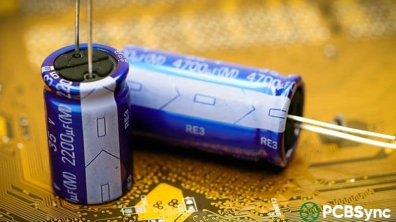
In modern EDA tools, a schematic symbol for a capacitor is separated from its physical footprint and the specific component part data. This three-layer model (Symbol → Component → Footprint) means the same generic “polarized capacitor” symbol can drive hundreds of different real parts — from a 10µF 6.3V X5R 0402 MLCC to a 4700µF 35V aluminium electrolytic — by changing the component attributes rather than redrawing the symbol.
KiCad’s standard library provides generic capacitor symbols (C for non-polarized, CP for polarized) with no footprint attached by default, allowing the engineer to assign the appropriate footprint later. Altium Designer provides similar generic symbols in its standard library, with the ANSI plate-style convention as default. Eagle uses both styles depending on library choice.
### Keeping Symbol Libraries Consistent
One practical consideration that rarely gets discussed in tutorials: if your team mixes IEC and ANSI-style symbols — perhaps because one engineer started the project with KiCad defaults and another imported symbols from an Altium library — the schematic becomes ambiguous. A polarized ANSI symbol and an IEC non-polarized symbol next to each other look similar to a casual reviewer. Establish which standard your team uses, create or curate a single symbol library source, and enforce it in design reviews.
IEC 60617 Database — The official IEC graphical symbols database, searchable online. Includes the authoritative definitions for all IEC capacitor symbol variants. Free basic access; subscription for full access
IEEE Std 315 (ANSI Y32.2) — The definitive US standard for electronic graphic symbols; purchasable from IEEE
EDA Component Libraries
SnapMagic (SnapEDA) — Free schematic symbols, PCB footprints, and 3D models for millions of components; exports to KiCad, Altium, OrCAD, Allegro, Eagle, and more. Start here when you need a manufacturer-specific symbol
UltraLibrarian — Similar to SnapMagic; strong coverage of capacitor manufacturers including Murata, TDK, KEMET, and Vishay
KiCad Official Libraries — Open-source symbol library built into KiCad; the Device library contains generic C, CP, C_Small, and CP_Small symbols
Murata SimSurfing — Simulate frequency response of real Murata capacitors to verify your circuit behaves as the schematic implies
## 5 FAQs About Capacitor Symbols
Q1: In a schematic, which plate of the polarized capacitor symbol is positive — the curved one or the straight one?
The straight plate is always positive and the curved plate is always negative, in both ANSI/IEEE and IEC 60617 conventions. This holds for aluminium electrolytic, tantalum, niobium, and any other polarized capacitor type. The curved plate is sometimes described as a “bent minus sign” — a visual mnemonic for its negative identity. Many engineers add an explicit “+” text annotation next to the straight plate as redundancy, which is good practice especially in dense schematics where the plate curvature can be hard to distinguish at small scale. Some CAD tools draw both plates as straight lines and rely entirely on the “+” annotation for polarity — this is valid under ANSI convention. In that case, the presence of a “+” sign, not the plate shape, is your polarity indicator.
Q2: Why does my KiCad schematic look different from the Texas Instruments reference design I’m copying from?
KiCad’s default capacitor symbols follow an IEC-influenced style, while TI and most US semiconductor company reference designs are drawn in ANSI/IEEE style. The functional meaning is identical — non-polarized is non-polarized, polarized is polarized — but the graphical style differs: IEC uses rectangular bar plates, ANSI uses thin line plates; IEC polarized symbols tend to rely more on the “+” annotation while ANSI relies more on plate curvature for the negative indicator. Neither is wrong. The confusion arises from mixing the two styles in the same schematic. For a design that follows a TI reference schematic, consider using ANSI-style symbols throughout to maintain visual consistency with your reference material — it makes design review against the reference easier. Most EDA tools let you import symbols from different libraries or create custom symbols that match whichever convention you want.
Q3: My schematic has a capacitor with an arrow through it — what does that mean?
That is a variable capacitor symbol. A diagonal arrow overlaid on a non-polarized capacitor symbol indicates that the capacitance value is adjustable. If the arrow is T-shaped, bent, or the symbol is annotated “Tr”, it’s a trimmer capacitor — adjustable during calibration but not intended for routine user adjustment. Variable capacitors are used in RF circuits for manual tuning (think of the tuning knob on an analog radio). Trimmer capacitors are used for factory calibration or field-adjustment of oscillator frequencies, filter corner frequencies, or impedance matching networks. The functional distinction between the two is one of adjustment intent, not of circuit topology: both are capacitors whose value can be changed mechanically. In a BOM, variable capacitors and trimmers will have distinct part numbers from fixed capacitors; the symbol variant tells the reader to look for an adjustable component, not a fixed value in picofarads.
Q4: Can I use the same capacitor symbol for an electrolytic and an MLCC on the same schematic?
You can use the same symbol type (polarized for electrolytic, non-polarized for MLCC) but the symbols are intentionally different for good reason. An MLCC is non-polarized and uses the two-equal-plate symbol. An aluminium electrolytic is polarized and uses the curved-plate symbol. Using the polarized symbol for an MLCC would imply a polarity requirement that doesn’t exist, potentially causing an assembler to try to orient the ceramic in a specific direction (which for an MLCC makes no functional difference but wastes time and could cause confusion). Using the non-polarized symbol for an electrolytic, on the other hand, removes the polarity warning that is critical for safe assembly. Use the correct symbol type for the component type, always. The dielectric type, package, and specific capacitance are in the component fields and BOM; the symbol carries the functional polarity information.
Q5: What do “X1”, “X2”, “Y1”, “Y2” annotations on a capacitor symbol mean?
These annotations indicate safety-rated capacitors used in mains-connected EMI filter circuits. X capacitors are connected line-to-line (across the mains) and Y capacitors are connected line-to-earth. The numbers (1 and 2) indicate the safety class and therefore the rated impulse voltage withstand. X1 capacitors handle impulse voltages above 2.5kV; X2 handles up to 2.5kV. Y1 capacitors handle impulse voltages above 8kV (double-insulated applications); Y2 handles up to 8kV. On a schematic, these parts typically appear with their reference designator named CX1, CX2, CY1, or CY2 (rather than just C) and carry the X/Y annotation next to the standard capacitor symbol — both the designator naming and the annotation alert the reviewer that a specifically safety-rated component is required in that position. Substituting a standard ceramic disc capacitor in an X or Y position is a safety violation, regardless of whether it has the correct capacitance value.
## Putting It Together: Schematic Best Practices for Capacitor Symbols
Choose one standard (ANSI/IEEE or IEC) and apply it consistently across the entire schematic. For new designs, IEC 60617 is the better long-term choice for international projects since it’s the international standard and most globally-distributed EDA libraries default to it. For designs that closely follow US semiconductor reference schematics, ANSI/IEEE keeps visual alignment with your source material.
Always use the correct symbol type — polarized for electrolytics and tantalums, non-polarized for ceramics, mica, and film. Include “+” annotations on all polarized symbols, especially for SMD tantalums where the physical polarity marking reversal is a known assembly trap. Annotate voltage ratings on all polarized capacitors in the schematic, not just in the BOM. Add silkscreen polarity markers to the PCB layout for every polarized capacitor footprint, and cross-reference polarity in the assembly drawing. These are not merely bureaucratic steps — they are the practical line between a first-pass success and a field return.
Inquire: Call 0086-755-23203480, or reach out via the form below/your sales contact to discuss our design, manufacturing, and assembly capabilities.
Quote: Email your PCB files to Sales@pcbsync.com (Preferred for large files) or submit online. We will contact you promptly. Please ensure your email is correct.
Notes: For PCB fabrication, we require PCB design file in Gerber RS-274X format (most preferred), *.PCB/DDB (Protel, inform your program version) format or *.BRD (Eagle) format. For PCB assembly, we require PCB design file in above mentioned format, drilling file and BOM. Click to download BOM template To avoid file missing, please include all files into one folder and compress it into .zip or .rar format.


