Inquire: Call 0086-755-23203480, or reach out via the form below/your sales contact to discuss our design, manufacturing, and assembly capabilities.
Quote: Email your PCB files to Sales@pcbsync.com (Preferred for large files) or submit online. We will contact you promptly. Please ensure your email is correct.
Notes: For PCB fabrication, we require PCB design file in Gerber RS-274X format (most preferred), *.PCB/DDB (Protel, inform your program version) format or *.BRD (Eagle) format. For PCB assembly, we require PCB design file in above mentioned format, drilling file and BOM. Click to download BOM template To avoid file missing, please include all files into one folder and compress it into .zip or .rar format.
Capacitor Impedance: Capacitive Reactance & AC Circuit Analysis
Pick up almost any AC circuit problem and a capacitor is involved — whether you’re designing a filter, selecting a bypass cap, troubleshooting a power supply oscillation, or building an RF matching network. In every case, the key parameter is capacitor impedance: how much the capacitor opposes current flow at a given frequency, and at what angle that opposition is shifted relative to the driving voltage.
This guide covers the complete picture: the capacitive reactance formula and its derivation, how reactance becomes complex impedance in AC analysis, phase relationships, the RC impedance triangle, and the real-world impedance model that governs capacitor behaviour above a few megahertz. Written for working PCB engineers and electronics designers who need to use these equations, not just cite them.
## Why Capacitors Behave Differently in AC vs DC Circuits
In DC steady state, a capacitor is an open circuit. Once fully charged, no current flows through it — the voltage across the plates equals the supply voltage and the current drops to zero. This is why capacitors block DC.
In AC circuits, the applied voltage is continuously reversing polarity. The capacitor never reaches a stable charged state because the voltage direction changes before it can finish charging. Instead, it continuously charges and discharges in response to the alternating voltage, and this continuous charging current constitutes an apparent current through the circuit. The faster the voltage alternates (higher frequency), the less time the capacitor has to charge in any given half-cycle, and the more current flows for a given voltage — so the opposition to current flow is lower. This inverse relationship between frequency and opposition is the defining characteristic of capacitive reactance.
## Capacitive Reactance: The Formula and What It Means
Capacitive reactance (symbol XC, unit: ohms, Ω) quantifies a capacitor’s opposition to alternating current at a specific frequency. The formula is:
XC = 1 / (2π × f × C)
Where:
XC = capacitive reactance in ohms (Ω)
f = frequency in hertz (Hz)
C = capacitance in farads (F)
2πf = ω, the angular frequency in radians per second (rad/s)
In angular frequency notation: XC = 1 / (ωC)
### Deriving the Formula from the Capacitor i-v Relationship
The derivation starts from the fundamental capacitor relationship I = C × dV/dt. Apply a sinusoidal voltage V(t) = Vm × sin(ωt) across the capacitor:
I(t) = C × d/dt[Vm × sin(ωt)] = C × Vm × ω × cos(ωt) = (ωCVm) × cos(ωt)
The peak current is Im = ωC × Vm. Rearranging for the ratio of peak voltage to peak current (which has units of ohms):
Vm/Im = 1/(ωC) = XC
This is Ohm’s Law for capacitive reactance: the “resistance” to AC current at frequency ω is XC = 1/(ωC).
### How XC Changes with Frequency
The inverse relationship between XC and frequency is fundamental and worth internalising with concrete numbers:
Capacitive Reactance vs. Frequency for Common Values:
Frequency
10nF Ceramic
100nF Ceramic
1µF Film
10µF Electrolytic
100µF Electrolytic
10 Hz
1,591 kΩ
159 kΩ
15.9 kΩ
1,591 Ω
159 Ω
100 Hz
159 kΩ
15.9 kΩ
1,591 Ω
159 Ω
15.9 Ω
1 kHz
15.9 kΩ
1,591 Ω
159 Ω
15.9 Ω
1.59 Ω
10 kHz
1,591 Ω
159 Ω
15.9 Ω
1.59 Ω
0.159 Ω
100 kHz
159 Ω
15.9 Ω
1.59 Ω
0.159 Ω
0.016 Ω
1 MHz
15.9 Ω
1.59 Ω
0.159 Ω
0.016 Ω
0.0016 Ω
10 MHz
1.59 Ω
0.159 Ω
0.016 Ω
0.0016 Ω
—
At DC (f = 0): XC → infinity (open circuit). At high frequency (f → ∞): XC → 0 (short circuit). This is what makes capacitors useful as coupling elements (pass AC, block DC) and as bypass and filter components (short-circuit noise to ground at high frequencies while presenting high impedance at low frequencies or DC).
## From Reactance to Complex Impedance: Z = −j/ωC
Reactance tells you the magnitude of a capacitor’s opposition to AC. Impedance goes further — it captures both the magnitude and the phase relationship between voltage and current. This is where complex number representation becomes necessary for proper AC circuit analysis.
### The Phase Relationship: Current Leads Voltage by 90°
From the derivation above, if V(t) = Vm × sin(ωt), then I(t) = ωCVm × cos(ωt). The cosine leads the sine by 90°, which means the current through a capacitor leads the voltage across it by 90°. The classic mnemonic is ICE (I before E in a Capacitor) — current (I) leads voltage (E) in a capacitive circuit.
This 90° phase lead is not just a mathematical curiosity. It has direct consequences for power calculation (reactive vs real power), impedance matching, and filter behaviour. In a purely capacitive circuit, average power consumption is zero because the current and voltage are 90° out of phase — power flows into the capacitor during one quarter-cycle and returns to the source during the next.
### Complex Impedance of an Ideal Capacitor
In the complex plane, the 90° phase angle is represented by the imaginary unit j (where j² = −1). The complex impedance of an ideal capacitor is:
ZC = −j × XC = −j / (ωC) = 1 / (jωC)
The negative sign in front of j places the capacitor’s impedance in the fourth quadrant of the complex impedance plane — it is a negative imaginary quantity. This is the opposite of an inductor, whose impedance is +jXL (positive imaginary, second quadrant).
In polar form: ZC has magnitude |ZC| = XC = 1/(ωC) and phase angle = −90°.
Impedance of Common Circuit Elements — Comparison:
Component
Impedance (Complex)
Magnitude
Phase Angle
Frequency Dependence
Ideal resistor
Z = R
R
0°
None
Ideal capacitor
Z = −j/(ωC) = 1/(jωC)
1/(ωC)
−90°
Inversely proportional to f
Ideal inductor
Z = jωL
ωL
+90°
Directly proportional to f
Series RC
Z = R − j/(ωC)
√(R² + XC²)
−arctan(XC/R)
Varies with f
Parallel RC
Z = R/(1+jωRC)
R/√(1+(ωRC)²)
−arctan(ωRC)
Varies with f
### The RC Impedance in Series Circuits
When a resistor R is in series with a capacitor C, the total impedance is:
Z = R + ZC = R − j/(ωC) = R − jXC
The magnitude (what a standard impedance meter measures) is:
|Z| = √(R² + XC²)
The phase angle (how far current leads voltage in the RC circuit) is:
φ = −arctan(XC / R)
This is the impedance triangle: resistance R along the horizontal axis, capacitive reactance XC pointing downward on the vertical axis (negative imaginary), and impedance magnitude |Z| as the hypotenuse. As frequency increases, XC decreases, the triangle “flattens” toward the horizontal (more resistive), and the phase angle approaches 0°. As frequency decreases, XC grows, the triangle elongates vertically, and the phase angle approaches −90°.
## Worked Examples: Calculating Capacitor Impedance
### Example 1: Single Capacitor Reactance
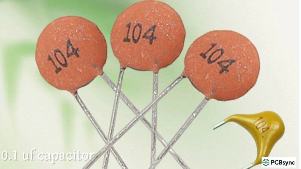
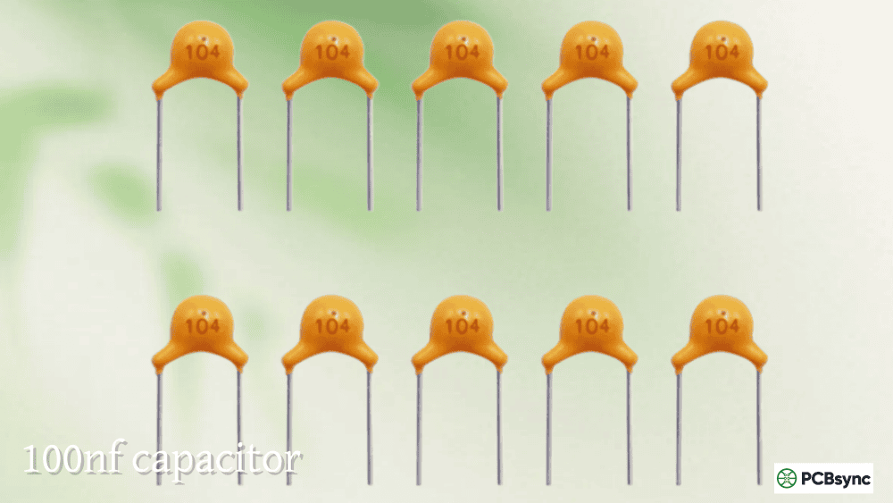
What is the impedance of a 100nF capacitor at 1kHz and at 10MHz?
The 100nF capacitor presents a high impedance (essentially open circuit) at 1kHz but near-zero impedance at 10MHz — which is why 100nF is a standard choice for high-frequency decoupling on IC power pins.
### Example 2: Series RC — Filter Corner Frequency and Impedance
A 10kΩ resistor in series with a 10nF capacitor. Find the total impedance and phase angle at 1kHz (below cutoff) and at 1.592kHz (the corner frequency).
The −3dB cutoff frequency is: fc = 1/(2πRC) = 1/(2π × 10,000 × 10×10⁻⁹) = 1,592 Hz
At the corner frequency, resistance equals reactance, phase angle is exactly −45°, and total impedance magnitude is R × √2. This is the mathematically clean condition that defines the −3dB point of an RC low-pass filter.
### Example 3: Finding Capacitor Value from Impedance Requirement
A bypass capacitor must present less than 1Ω of impedance at 100MHz. What minimum capacitance is needed?
XC < 1 Ω → 1/(2π × 100×10⁶ × C) < 1 → C > 1/(2π × 100×10⁶) → C > 1.59nF
In practice, a 10nF or 100nF MLCC would easily meet this requirement for an ideal capacitor. The limiting factor in real designs, as discussed below, becomes the parasitic inductance (ESL) rather than the capacitance value.
Worked Examples Summary:
| Scenario | Component Values | Frequency | XC | |Z| | Phase | |—|—|—|—|—|—| | Bypass cap check (low f) | C = 100nF | 1 kHz | 1,591 Ω | 1,591 Ω | −90° | | Bypass cap check (high f) | C = 100nF | 10 MHz | 0.159 Ω | 0.159 Ω | −90° | | RC filter at corner frequency | R=10kΩ, C=10nF | 1,592 Hz | 10,000 Ω | 14,142 Ω | −45° | | RC filter below cutoff | R=10kΩ, C=10nF | 1 kHz | 15,915 Ω | 18,847 Ω | −57.9° | | Min bypass cap for <1Ω at 100MHz | Any MLCC | 100 MHz | <1 Ω | — | Need C >1.59nF |
## The Real Capacitor Impedance Model: ESR, ESL, and Self-Resonant Frequency
The ideal capacitor model ZC = 1/(jωC) is accurate at low and moderate frequencies but breaks down in the megahertz range and above. Every real capacitor has parasitic elements that fundamentally change its impedance behaviour at high frequencies. For PCB engineers working on power distribution networks, RF circuits, or high-speed digital designs, this is not an academic detail — it determines whether your decoupling strategy works or fails.
### The Real Capacitor Equivalent Circuit
A real capacitor is modelled as a series RLC circuit:
Z_real = ESR + jωESL − j/(ωC)
Where:
ESR (Equivalent Series Resistance): the resistive loss from lead resistance, electrode resistance, and dielectric loss. Units: ohms. Represents real power dissipation.
ESL (Equivalent Series Inductance): the parasitic inductance from lead geometry, electrode traces, and current loop area. Units: henrys. Increases impedance at high frequencies.
C: the capacitance, as specified.
Rleakage: a very large shunt resistance (typically hundreds of megaohms to gigaohms) representing leakage through the dielectric; usually ignored in AC analysis.
### Self-Resonant Frequency (SRF)
Because the real capacitor model contains both capacitance C and inductance ESL, it has a self-resonant frequency where the capacitive and inductive reactances cancel:
SRF = 1 / (2π × √(ESL × C))
At the SRF, XC = XL (they cancel), and the impedance reaches its minimum value, which equals ESR. This is the frequency at which a real capacitor performs best as a bypass or filter element — lowest impedance, pure resistive character.
Below the SRF: the capacitor behaves capacitively (impedance decreases with rising frequency, as expected). Above the SRF: the ESL dominates and impedance rises with frequency — the capacitor is now behaving like an inductor, not a capacitor. Above its SRF, a bypass capacitor provides no filtering benefit whatsoever.
Typical ESR, ESL, and SRF Values by Capacitor Type:
### The Impedance Curve: The V-Shape That Every PCB Engineer Should Know
The impedance vs. frequency plot for a real capacitor has a characteristic V-shape on a log-log scale:
The left slope (below SRF) descends at −20 dB/decade — the capacitive region where XC = 1/(ωC) and impedance falls as frequency rises.
The bottom of the V is the SRF — the frequency of minimum impedance, equal to ESR.
The right slope (above SRF) ascends at +20 dB/decade — the inductive region where XL = ωESL and impedance rises as frequency rises.
A bypass capacitor only works in the region where it is capacitive — from very low frequency up to its SRF. Above that frequency, it becomes an inductor, and inductors block high-frequency current rather than bypassing it. Choosing a bypass cap without considering its SRF is one of the most common mistakes in PCB power distribution network (PDN) design.
## Practical Implications for PCB Design
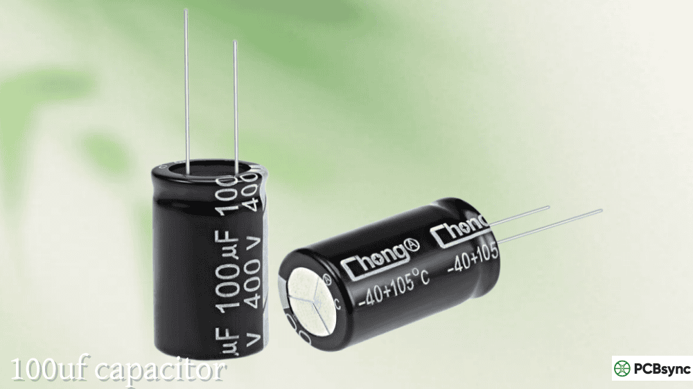
### Why “Bigger is Not Always Better” for Bypass Capacitors
At first glance, a 100µF bulk electrolytic seems like better decoupling than a 100nF ceramic. More capacitance, more charge stored, better filtering — right? Wrong, above a few hundred kilohertz. The 100µF electrolytic has a SRF of perhaps 400–700 kHz and several milliohms to hundreds of milliohms of ESR, while the 100nF MLCC in a 0402 package has a SRF around 15–20 MHz and ESR under 50mΩ. For a processor switching at 100MHz or higher, the electrolytic is above its SRF and is presenting inductive impedance — it’s making things worse, not better.
The industry-standard PDN strategy uses multiple capacitor values in parallel to cover the full frequency spectrum: a large bulk electrolytic (10–470µF) for low-frequency charge storage (below 1MHz), a mid-range capacitor (1–10µF X5R/X7R MLCC) for mid-frequency filtering, and small high-SRF ceramics (100nF 0402 or 0201) placed directly adjacent to IC power pins for high-frequency bypass.
### Package Size and ESL: Why Smaller is Better at High Frequency
ESL is determined largely by the current loop geometry: specifically the length of the current path through the component relative to its width. Smaller packages have shorter, wider electrode structures, giving lower ESL and therefore higher SRF. A 0201 MLCC has around 0.3–0.5nH ESL compared to ~2nH for a 0805 of the same capacitance — giving an SRF roughly 2× higher for the same capacitance. For decoupling above 500MHz, 0201 or even 01005 packages are preferred precisely for this reason.
Mounting inductance — the inductance of the PCB pads, vias, and traces connecting the capacitor to the power rail — also adds to the effective total series inductance. A typical via can add 0.4–0.8nH. Placing bypass capacitors as close as possible to the IC power pin, with short traces to both power and ground vias, minimises the mounting inductance and keeps the effective SRF as high as possible.
## Complete Formula Reference for Capacitor Impedance
Murata SimSurfing — Simulates actual impedance vs. frequency curves for Murata MLCCs using manufacturer S-parameter data; the most accurate tool for real capacitor impedance
Q1: What is the difference between capacitive reactance XC and capacitor impedance Z — aren’t they the same thing?
Reactance and impedance both measure opposition to current in ohms, but they are not the same thing. Reactance (XC) is a scalar quantity that describes the magnitude of a capacitor’s opposition to AC at a given frequency, without reference to phase. Impedance (Z) is a complex quantity that captures both the magnitude and the phase angle of the opposition. For an ideal capacitor: XC = 1/(ωC) and ZC = −jXC. The −j factor is what encodes the 90° phase shift between current and voltage. In circuit analysis, you need the full complex impedance Z when dealing with circuits that mix resistors and capacitors, because the phase relationships determine how voltages and currents add — they don’t add arithmetically when the phases differ. In a practical calculation for an RC filter or matching network, ZC = −j/(ωC) is what you use in the circuit equations; XC is the magnitude you’d read on an impedance meter or quote in a spec.
Q2: My datasheet shows that a 1µF capacitor has only 0.3Ω of impedance at 10MHz — but my circuit doesn’t filter well at that frequency. What’s going wrong?
The most likely culprit is that your capacitor is above or near its self-resonant frequency (SRF) at 10MHz, or that the mounting inductance is pushing the effective SRF lower than the datasheet value. A 1µF MLCC with 1nH ESL has a SRF of approximately 1/(2π√(1nH × 1µF)) ≈ 5MHz. At 10MHz it’s operating above its SRF and presenting inductive impedance — not capacitive. The 0.3Ω figure you see might be the impedance at the SRF minimum, not at 10MHz. Check the manufacturer’s impedance vs. frequency curve (Murata’s SimSurfing and TDK’s product database provide these). If you need effective filtering at 10MHz with 1µF, you either need a higher-SRF component (lower ESL — use smaller package, reverse-geometry MLCC, or multiple 100nF in parallel) or you need to accept that the 1µF is handling lower frequencies while smaller-value caps handle the 10MHz range.
Q3: In an RC series circuit, when I add more capacitance does the impedance go up or down, and does this change the phase angle?
Adding more capacitance (larger C value) decreases XC at any given frequency (since XC = 1/(ωC)), which decreases the total series impedance magnitude |Z| = √(R² + XC²). The phase angle φ = −arctan(XC/R) also moves closer to 0° — less capacitive, more resistive in character. This makes intuitive sense: a very large capacitor has almost zero reactance and the series RC circuit looks mostly like a resistor. Conversely, a very small capacitor has high reactance and the circuit looks mostly capacitive with φ approaching −90°. The cutoff frequency fc = 1/(2πRC) rises as C decreases (smaller cap → higher corner frequency), so selecting the capacitor value is essentially selecting where the transition from capacitive to resistive behaviour occurs in the frequency domain.
Q4: What does a negative phase angle mean in practical terms for my circuit?
A negative phase angle for capacitor impedance means the current through the capacitor leads the voltage across it — current peaks before voltage peaks in the sinusoidal waveforms. In a practical RC circuit, the phase angle of the impedance (−arctan(XC/R)) tells you the phase relationship between the total voltage applied to the circuit and the current flowing through it. This becomes important in power calculations: average power P = V × I × cos(φ), where φ is the phase angle. A purely capacitive circuit (φ = −90°) has cos(−90°) = 0 — zero average power, since the capacitor stores and returns energy without net dissipation. As R increases relative to XC (frequency rises or you add more resistance), the phase angle approaches 0° and real power dissipation increases. In AC mains power applications, this is the power factor issue — reactive loads (capacitive or inductive) draw current that contributes nothing to useful power, but still flows through the supply cables and causes I²R losses.
Q5: Why do engineers place two different capacitor values in parallel for bypassing — what does this achieve that a single larger capacitor doesn’t?
Two different capacitor values in parallel provide low impedance across a wider frequency range than either capacitor alone. A 100µF electrolytic is effective below its SRF (roughly 400–700kHz) but becomes inductive above that. A 100nF MLCC in a 0402 package has a SRF around 15–20MHz and provides low impedance from about 1MHz to 20MHz. In parallel, the combination covers both ranges. The key insight is that you cannot simply increase capacitance to push the SRF up — SRF = 1/(2π√(ESL × C)), and increasing C actually lowers SRF for a given ESL. The only way to achieve high-frequency decoupling is to use small-value, small-package capacitors with inherently low ESL. Parallel combinations of different values effectively create a flat-impedance power distribution network by having different capacitors “take over” at different frequencies. This is the basis of the multi-tier decoupling strategy used on any high-speed digital PCB: bulk capacitors for low frequencies, mid-range MLCCs for intermediate frequencies, and small-value 0402/0201 ceramics directly at the IC for high-frequency bypass.
## Putting Capacitor Impedance to Work
The capacitive reactance formula XC = 1/(2πfC) and its complex form ZC = −j/(ωC) are the starting point, but the real engineering begins when you recognise that these describe only an ideal component. Real capacitors have ESR, ESL, and a self-resonant frequency that defines where their useful operating range ends. Below the SRF, the component behaves as designed. Above it, it’s an inductor.
For AC circuit analysis below a few hundred kilohertz — filters, signal coupling, timing networks, audio circuits — the ideal model is entirely adequate. For power distribution networks in high-speed digital and RF designs, the full ESR+ESL model and the impedance-vs-frequency curve from the manufacturer’s datasheet are the essential tools. The capacitor that works perfectly at 100kHz may be completely ineffective at 100MHz, and understanding impedance is what tells you which one you have.
Inquire: Call 0086-755-23203480, or reach out via the form below/your sales contact to discuss our design, manufacturing, and assembly capabilities.
Quote: Email your PCB files to Sales@pcbsync.com (Preferred for large files) or submit online. We will contact you promptly. Please ensure your email is correct.
Notes: For PCB fabrication, we require PCB design file in Gerber RS-274X format (most preferred), *.PCB/DDB (Protel, inform your program version) format or *.BRD (Eagle) format. For PCB assembly, we require PCB design file in above mentioned format, drilling file and BOM. Click to download BOM template To avoid file missing, please include all files into one folder and compress it into .zip or .rar format.


